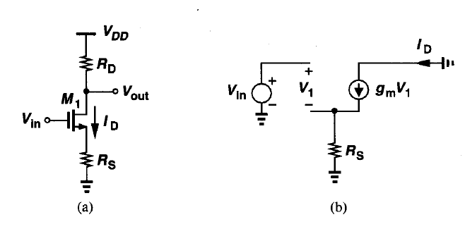
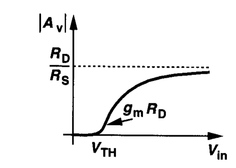
CS Stage
CS Stage With Resistive Load
电路图和小信号模型
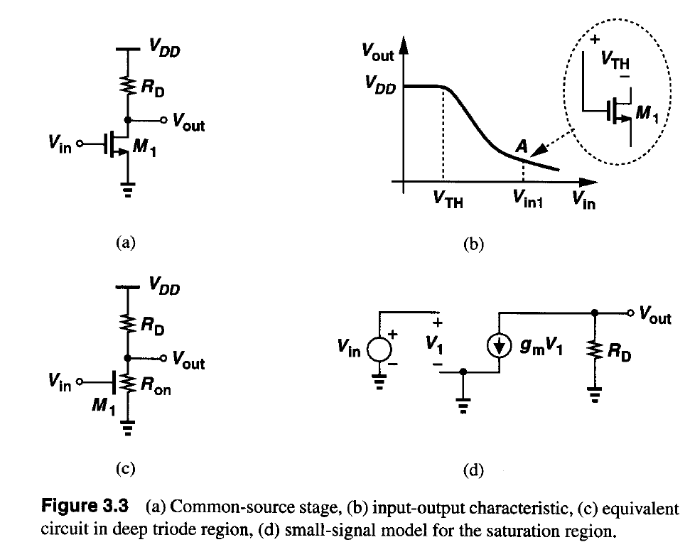
- $\pmb{V_{in} = V_{GS}}$
输入-输出关系 增益
- $V_{out} - V_{in}$
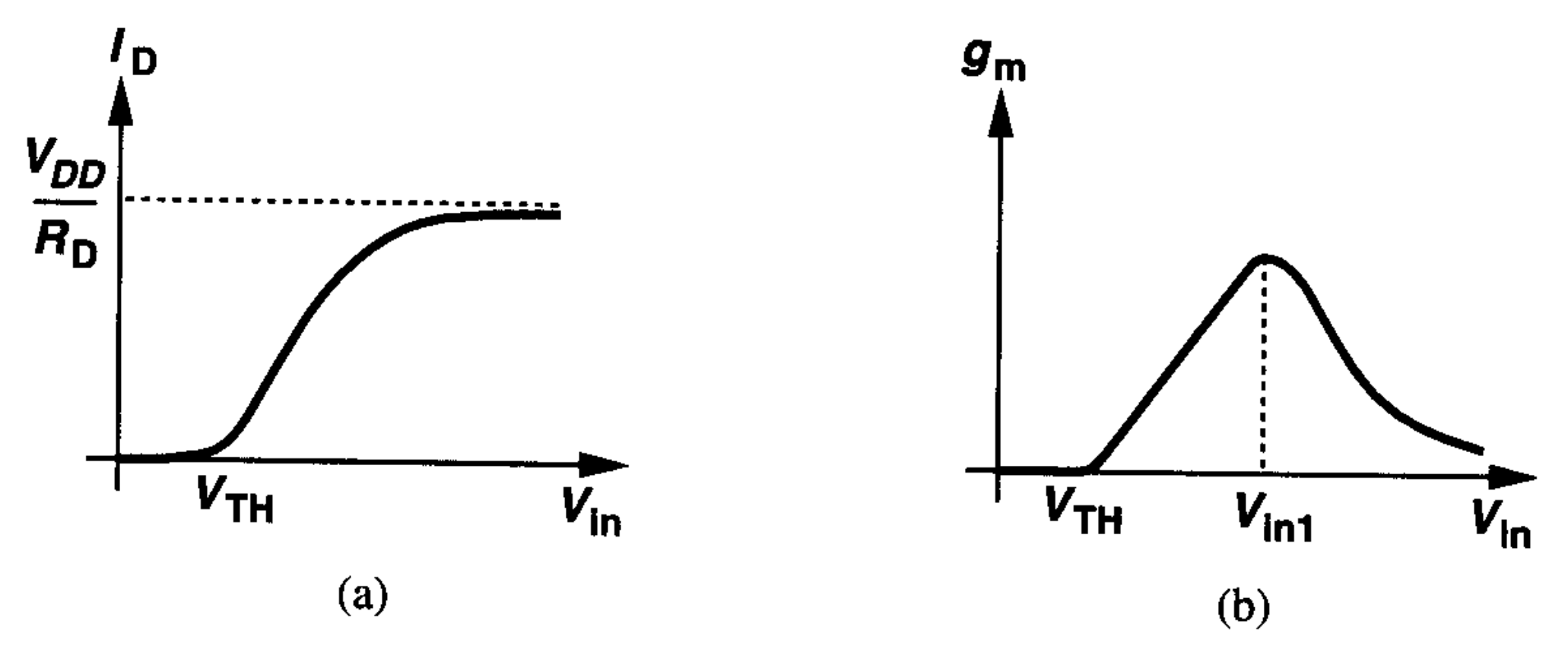
$$ V_{in} = V_{GS}, V_{out} = V_{DS} \\\ \\ V_{out} = \begin{cases} V_{DD} (没有压降) & V_{in} \lt V_t \\ V_{DD} -\frac{1}{2}k_n (V_{in} - V_t)^2 R_D & V_{in} \ge V_t \\ V_{in} - V_t & V_{in} - V_t = V_{out} \\ V_{DD} - \frac{1}{2}[2(V_{in} - V_t)V_{out}- V_{out}^2] R_D & Triode \ Region \end{cases} \\\ \\ 如果V_{in}很大,使得V_{out} \ll 2(V_{in} -V_t) \\\ \\ \begin{aligned} V_{out} &= \frac{R_{on}}{R_{on} + R_D}V_{DD} \\ &= \frac{V_{DD}}{1 + k_n R_D(V_{in} -V_t)} \\ ( R_{on} &= \frac{V_{out}}{i_D},i_D = k_nR_D(V_{in}-V_t)V_{out} ) \\\ \end{aligned} $$
- 增益
$$ \begin{equation} \begin{aligned} A_v &= \frac{ \partial V_{out} }{ \partial V_{in}} \\ &= -g_m R_D \end{aligned} \end{equation} $$
Important Relations
Gain Considering Channel Length Modulation
$$ \begin{aligned} V_{out} &= V_{DD} - \frac{1}{2}k_n(V_{in} - V_t)^2 (1 + \lambda V_{out})R_D \\ \therefore A_v &= \frac{\partial V_{out}}{\partial V_{in}}\\ &= - R_Dk_n (V_{in} - V_t)(1 + \lambda V_{out})- \frac{1}{2}k_n R_D(V_{in} - V_t)^2 \lambda\frac{\partial V_{out}}{\partial V_{in}} \\ &= -R_D g_m - I_DR_D \lambda A_v (近似) \\ &= -\frac{g_m R_D}{1 + R_D \lambda I_D} \\ &= -g_m \frac{r_0R_D}{r_0 + R_D} \end{aligned} $$
$$ \begin{equation} A_v = -g_m\frac{ r_o R_D}{ r_0 + R_D } \end{equation} $$
-
其中,$\lambda I_D = \dfrac{ 1 }{ r_0 }$
-
效果就是并联$r_0$和$R_D$作为输出电阻,$1/g_m$是输入电阻
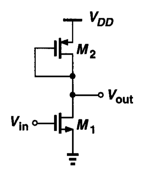
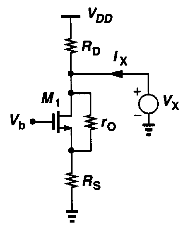
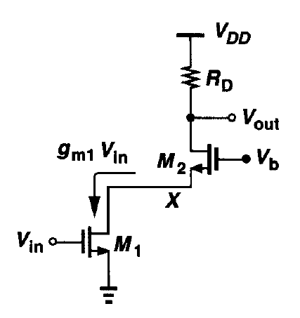
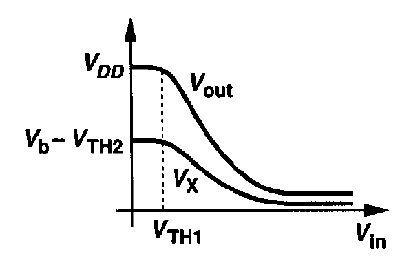
CS Stage With Diode-Connected Load
输入阻抗
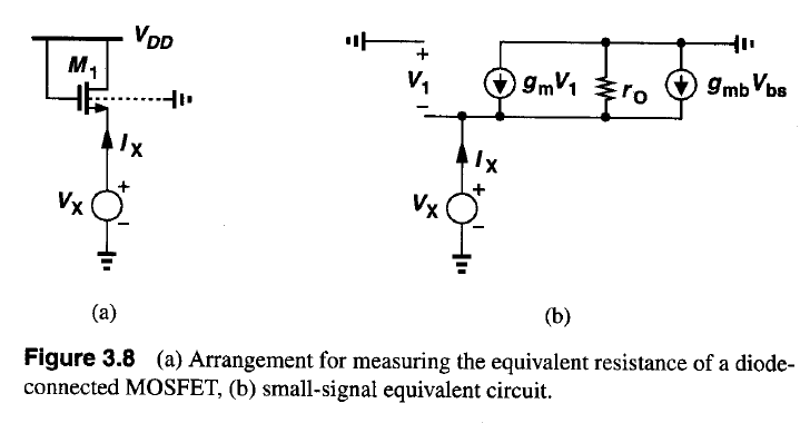
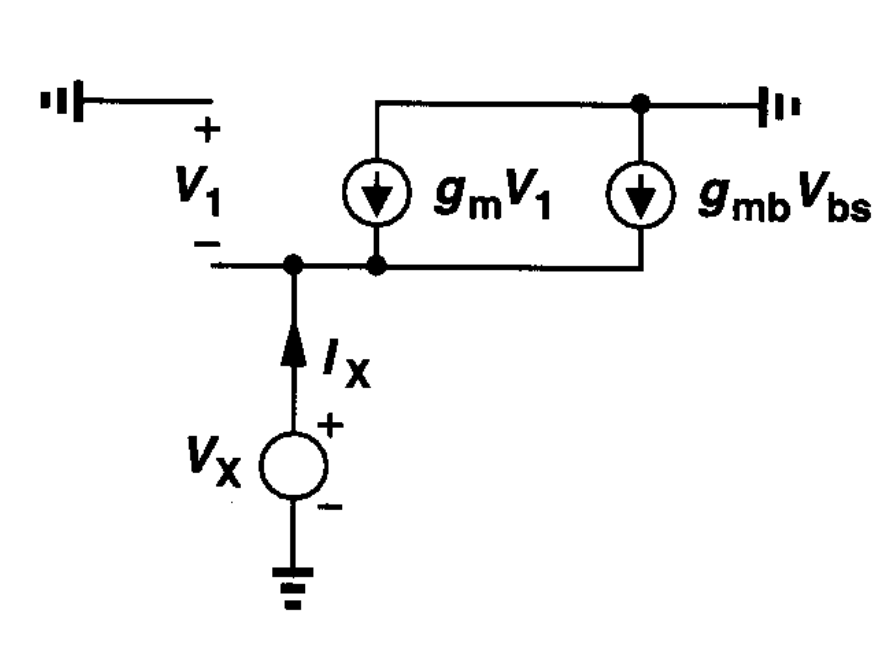
$$ \begin{aligned} V_1 &= V_{bs} = -V_X \\\ \\ I_X &=\frac{V_X}{r_0} + (g_m + g_{mb})V_X \\ \frac{V_X}{I_X} &= \frac{1}{g_m+g_{mb}+r_0^{-1}} \\ &= \frac{1}{g_m + g_{mb}} || r_0 \\ & \approx \frac{1}{g_m +g_{mb}} \\ Z_{in} &\approx \frac{1}{g_m + g_{mb}} \end{aligned} $$
增益
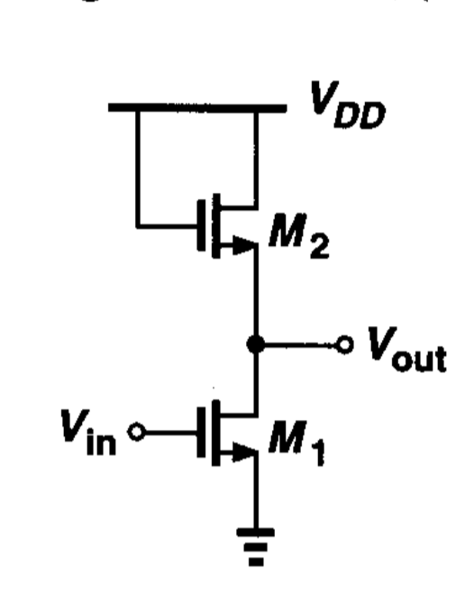
- Method I
$$ \begin{aligned} A_v &= -g_{m1} \frac{1}{g_{m2} + g_{mb2}} \\ &= -\frac{g_{m1}}{g_{m2}}\frac{1}{1 + \eta} \\ \because I_{D1} &= I_{D2} \\ \therefore A_v &= \frac{\sqrt{2k_nI_{D1}}}{\sqrt{2k_nI_{D2}}}\frac{1}{1+\eta} \end{aligned} $$
$$ \begin{equation} \begin{aligned} A_v &= -\sqrt{\frac{(W/L)_1}{(W/L)_2}}\frac{1}{1+\eta} \\ &\approx - \sqrt{ \frac{ (W/L)_1 }{ (W/L)_2 } } \end{aligned} \end{equation} $$
- 其中,$\pmb{\eta=\dfrac{g_{mb2}}{g_{m2}} = \dfrac{\partial V_{TH}}{\partial V_{out}}}$
- Method II
$$ \begin{aligned} I_{D1} &= I_{D2} \\ \frac{1}{2}k_{n1}(V_{in} - V_{t1})^2 &= \frac{1}{2}k_{n2}(V_{DD} - V_{out} -V_{t2})^2 \\ \sqrt{(\frac{W}{L})1} (V{in} -V_{t1}) &= \sqrt{(\frac{W}{L})2}(V{DD} - V_{out} - V_{t2}) \\ \sqrt{(\frac{W}{L})1} &= -\sqrt{(\frac{W}{L})2}(\frac{\partial V{out}}{\partial V{in}} - \frac{\partial V_{t2}}{\partial V_{in}}) \\ \because \frac{\partial V_{t2}}{\partial V_{in}} &= \frac{\partial V_{t2}}{\partial V_{out}} \frac{\partial V_{out}}{\partial V_{in}} = \eta\frac{\partial V_{out}}{\partial V_{in}} \\ \therefore A_v &= \frac{\partial V_{out}}{V_{in}} \\ &= -\sqrt{\frac{(W/L)_1}{(W/L)_2}}\frac{1}{1+\eta} \\ &\approx -\sqrt{\frac{(W/L)_1}{(W/L)_2}} \end{aligned} $$
- 总结
- 不考虑Channel-Length-Modulation和Body Effect的情况下,$A_v = 1$
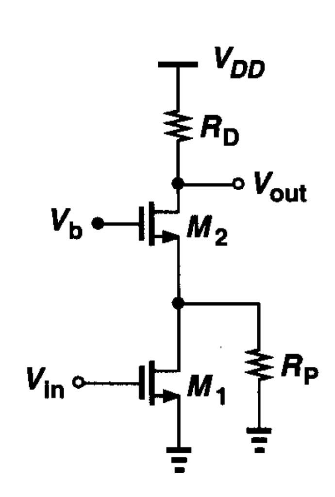
CS stage with diode-connected PMOS device
$$ \begin{aligned} \because I_{D1} & = I_{D2} \\ \therefore k_nV_{ovn}^2 &= k_pV_{ovp}^2 \\ \therefore \frac{\mu_n (W/L)n}{\mu_p(W/L)p} &= \frac{|V{ovp}|}{V{ovn}} \\ \therefore A_v &\approx -\frac{|V_{GS2} - V_{TH2}|}{V_{GS1} - V_{TH1}} \\ &\approx -\frac{k_n|V_{GS2} - V_{TH2}|}{V_{GS1} - V_{TH1}} \\ &\approx \frac{g_{mn}}{g_{mp}} \end{aligned} $$
- 在考虑现实因素的情况下
$$ \begin{equation} A_v = -g_{mn} (\frac{1}{g_{mp}} || r_{on} || r_{op}) \end{equation} $$
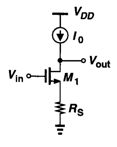
CS Stage With Current-Source Load
Gain
$$ \begin{equation} A_v = -g_m(r_{o1} || r_{o2}) \end{equation} $$
Intrinsic Gain
$$ \begin{equation} g_mr_o = \sqrt{2(\frac{W}{L})\mu_nC_{OX}I_D} \frac{1}{\lambda I_D} \end{equation} $$
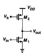
CS Stage With Triode Load
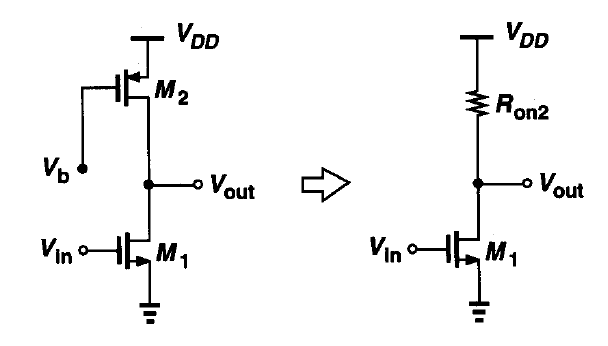
$$ \begin{equation} \begin{aligned} R_{on2} &= \frac{1}{g_{m2}} \\ &= \frac{1}{\mu_p C_{OX}(W/L)2(V{DD} -V_b-V_{Tp})} \end{aligned} \end{equation} $$
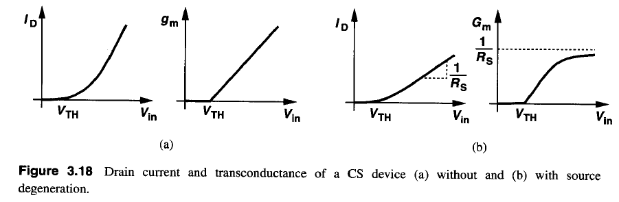
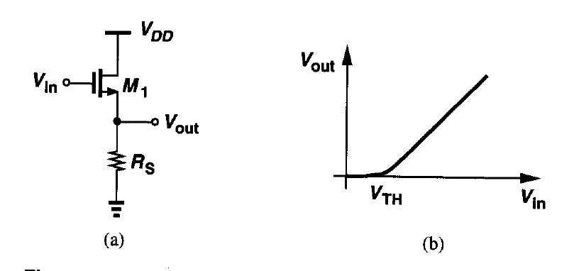
CS Stage With Source Degeneration
电路
简化分析 Gain
$$ 设I_D = f(V_{GS}) \\\ \\ \begin{aligned} G_m &= \frac{\partial I_D}{\partial V_{in}} \\ &= \frac{\partial f}{\partial V_{GS}}\frac{\partial V_{GS}}{\partial V_{in}} \\ &= g_m(\frac{ \partial (V_{in} - I_DR_S)}{\partial V_{in}}) \\ &= g_m (1-R_S\frac{\partial I_D}{\partial V_{in}}) \\ &= g_m(1 -R_SG_m) \\ \therefore G_m &= \frac{g_m}{1+g_mR_S} \\ &= \frac{1}{\dfrac{1}{g_m} + R_S} \end{aligned} $$
$$ \begin{equation} \begin{aligned} A_v &= -G_m R_D \\ &= -\frac{g_mR_D}{1 + g_mR_S} \end{aligned} \end{equation} $$
具体分析 Gain
- 考虑了Channel Length Modulation和Body Effect
- 小信号模型
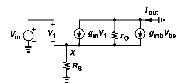
- 等效跨导
$$ \begin{aligned} I_{out} &= g_mV_1 - \frac{I_{out} R_S}{r_O} -g_mV_X \\ &= g_m (V_{in} - I_{out} R_S) - \frac{I_{out}R_S}{r_O} + g_m (-I_{out}R_S) \\ G_m &= \frac{I_{out}}{V_{in}} \\ &= \frac{g_mr_o}{R_S + [1 + (g_m + g_{mb})R_S]r_O} \end{aligned} \\\ $$
- 增大的输出电阻
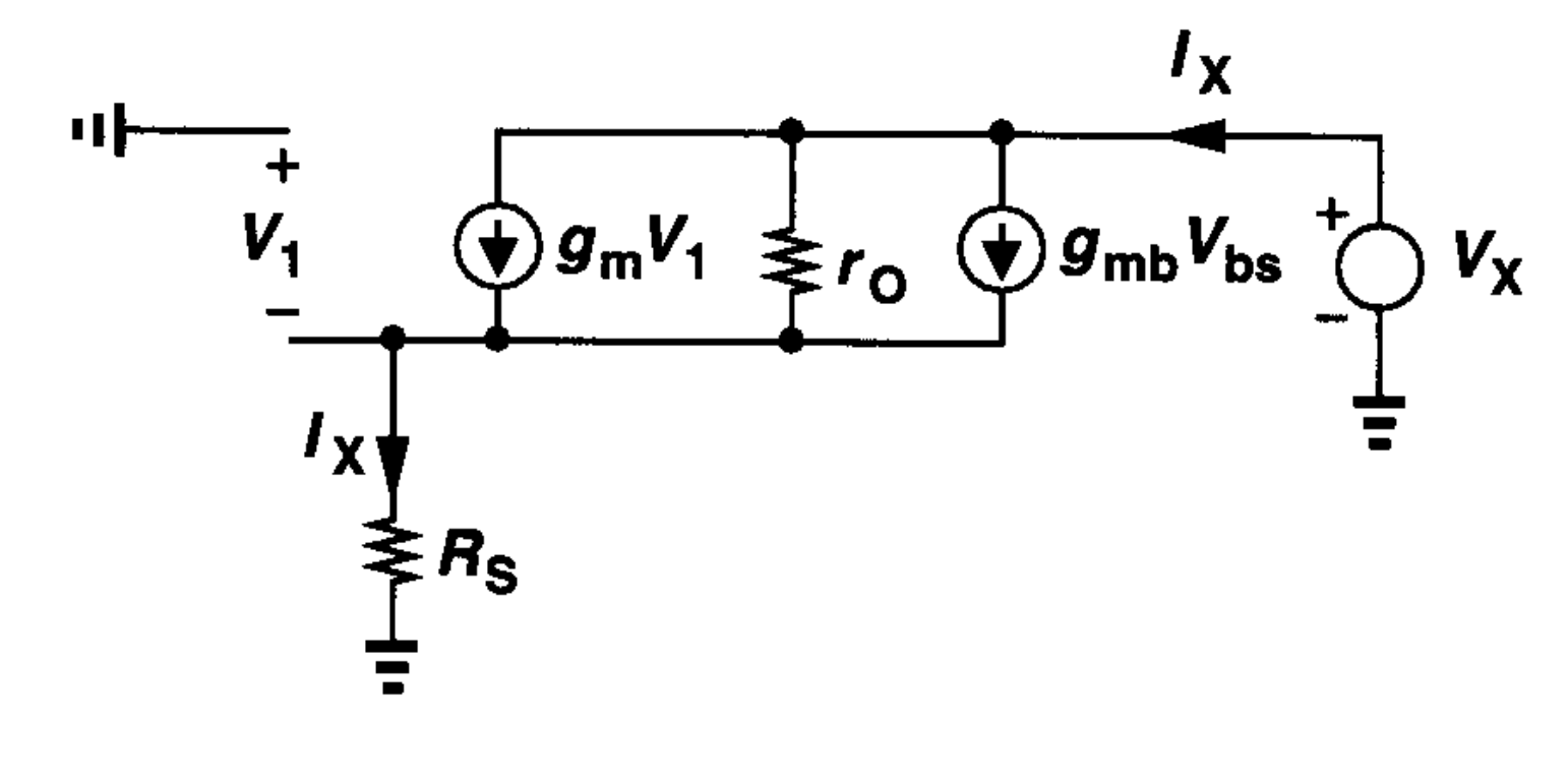
$$ \begin{aligned} I_{ro} &= I_X - g_m(V_1 + V_{bs}) \\ V_1 &= - I_XR_S \\ \therefore V_X &= I_{ro} r_o + I_X R_S \\ \therefore R_{out} &= \frac{V_X}{I_X} \\ &= R_S + [1 + (g_m + g_{mb}) R_S]r_o \end{aligned} $$
- 最终增益
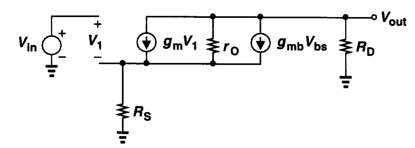
$$ \begin{aligned} A_v &= \frac{V_{out}}{V_{in}} \\ &= -\frac{g_m r_o R_D}{R_D + R_S + r_o + (g_m + g_{mb}) R_S r_o} \end{aligned} $$
图像
CS Stage With Source Degeneration & Constant Current Source
$$ \begin{aligned} A_v &= -g_m r_o \end{aligned} $$
- 这种情况下,通过$R_S$的$AC$电流为0
Source Follower
电路 电压特性
Gain
- 只考虑Body Effect
$$ \begin{aligned} V_{out} &= \frac{1}{2}k_n(V_{in} -V_{out} -V_t) ^2 R_S \\ \frac{\partial V_{out}}{\partial V_{in}} &= k_n(V_{in}- V_{out} -V_t) (1 - \frac{\partial V_{out}}{\partial V_{in}} - \frac{\partial V_t}{\partial V_{in}}) R_S \\ \because \frac{\partial V_t}{\partial V_{in}} &= \eta \frac{\partial V_{out}}{\partial V_{in}} \\ \therefore \frac{\partial V_{out}}{\partial V_{in}} &= \frac{k_nV_{OV}R_S}{1+k_nV_{OV}R_S(1 +\eta)} \\ \because g_m &= k_nV_{OV} \end{aligned} $$
$$ \begin{equation} A_v = \frac{g_m R_S}{1 + (g_m + g_{mb}) R_S} \end{equation} $$
- 若不考虑Body Effect,$A_v = \dfrac{1}{\dfrac{1}{g_m} + R_S} R_S$, 和CS Degeneration十分相似
输出电阻
- 只考虑Body Effect
$$ \begin{aligned} V_X &= - V_1 = -V_{bs}\\ I_X &= g_mV_1 + g_{mb} V_{bs} \\ \therefore R_{out} &= \frac{V_X}{I_X} \\ &= \frac{1}{g_m + g_{mb}} \\ &= \frac{1}{g_m} || \frac{1}{g_{mb}} \end{aligned} $$
Source Follower Driving Resistive Load
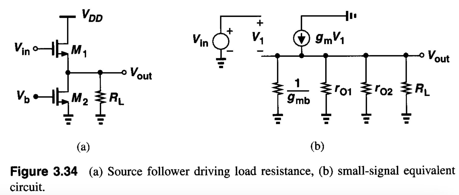
- 考虑了CLM和Body Effect
$$ \begin{aligned} A_v &= \frac{\dfrac{1}{g_{mb}} || r_{o1} || r_{o2} || R_L }{\dfrac{1}{g_{mb}} || r_{o1} || r_{o2} || R_L + \dfrac{1}{g_m}} \end{aligned} $$
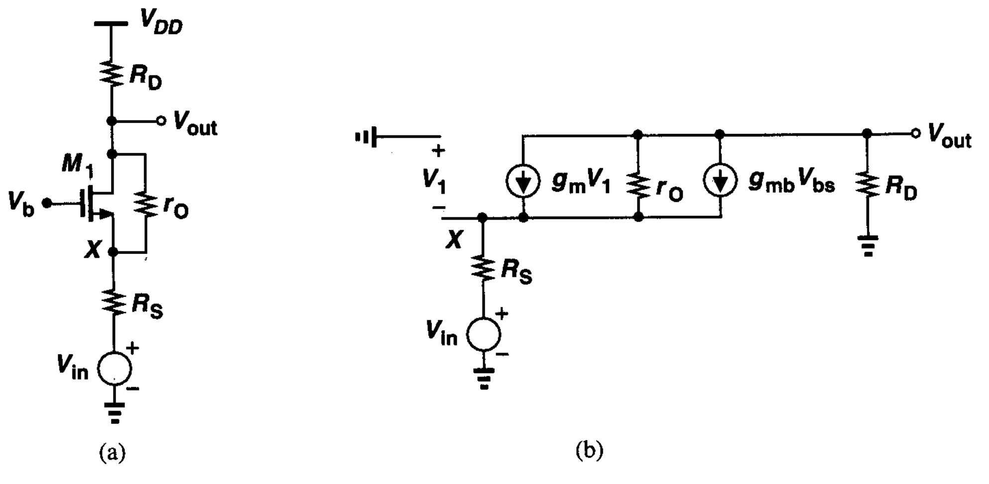
Common-Gate Stage
电路
-
(a) 直接耦合
-
(b) 电容耦合
Gain
简化后的 Gain
$$ \begin{aligned} V_{out} &= V_{DD} - \frac{1}{2}k_n(V_b -V_{in} -V_t)^2R_D \\ \therefore A_v &= \frac{\partial V_{out}}{\partial V_{in}} \\ &= -k_nV_{OV}(-1-\eta) R_D \\ &= g_m R_D ( 1 + \eta) \end{aligned} $$
$$ \begin{equation} A_v = g_m R_D \end{equation} $$
普适性的Gain
$$ \begin{aligned} V_1 - \frac{V_{out}}{R_D} R_S + V_{in} &=0 \\ V_{out} &=V_{in} -\frac{V_{out}}{R_D} R_S + (V_1(g_m + g_{mb}) - \frac{V_{out}}{R_D})r_o \end{aligned} $$
$$ \begin{equation} A_v =\frac{V_{out}}{V_{in}} = \frac{1 + (g_m + g_{mb})r_o }{r_o + (g_m + g_{mb})r_oR_S + R_S +R_D}R_D \end{equation} $$
- 若 $R_D \rightarrow \infin$
$$ \begin{equation} A_v = 1 + (g_m + g_{mb}) r_o \end{equation} $$
Impedence
Input Impedence
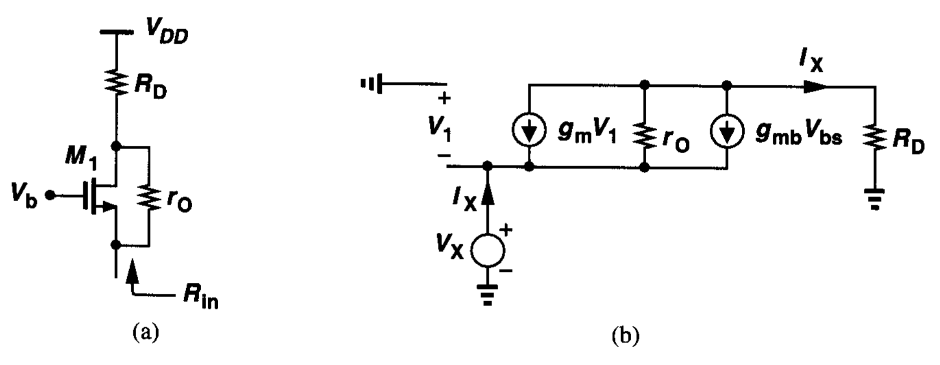
$$ \begin{aligned} V_1 &= -V_X \\ V_X + (g_mV_1 + g_{mb}V_{bs} - I_X)r_o &= I_XR_D \\ \therefore R_{in} &= \frac{V_X}{I_X} \\ &= \frac{R_D + r_o}{1 + (g_m + g_{mb})r_o} \end{aligned} $$
- 因为$(g_m + g_{mb})r_o \gg 1$
$$ \begin{equation} R_{in }\approx \frac{R_D}{(g_m + g_{mb})r_o} + \frac{1}{g_m + g_{mb}} \\ \end{equation} $$
- 若$R_D = 0$
$$ \begin{equation} R_{in} = \frac{1}{g_m + g_{mb} + \dfrac{1}{r_o}} \end{equation} $$
Output Impedence
$$ \begin{equation} R_{out} = \big[ (1 + (g_m + g_{mb})r_o)R_S + r_o \big] || R_D \end{equation} $$
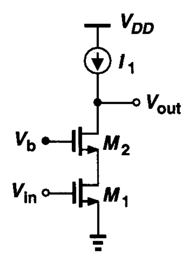
Cascode Stage
Basic Configuration
电路
-
CS + CG
-
$M_1$: Input Device
-
$M_2$: Cascode Device
Voltage Range
- 为了让$M_1$工作在Saturation Region
$$ \begin{aligned} V_X &\ge V_{in} - V_{T1} \\ V_X &= V_b - V_{GS2} V_b -V_{GS2} &\ge V_{in} -V_{T1} \\ V_b &\ge V_{in} - V_{T1} + V_{GS2} \end{aligned} $$
- 为了让$M_2$工作在Saturation Region
$$ \begin{aligned} \\ V_{out} - V_{S2} &\ge V_b - V_{S2} - V_{T2} \\ V_{out} &\ge V_b - V_{T2} (4)\\ V_{out} &\ge (V_{in} - V_{T1}+ V_{GS2} -V_{T2}) \\ \end{aligned} $$
$$ \begin{equation} V_{b \ min} = V_{in} - V_{TH1} + V_{GS2} \end{equation} $$
$$ \begin{equation} V_{out \ min} = V_{OV1} + V_{OV2} \end{equation} $$
I/O 特性
Cascode Stage With a Source Resistance
$$ \begin{aligned} I_{D2} &= I_{D1} \frac{R_p}{\dfrac{1}{g_m + g_{mb}} + R_p} \\ &= g_{m1} V_{in} \frac{(g_m + g_{mb})R_p}{1 + (g_m + g_{mb})R_p} \end{aligned} $$
$$ \begin{equation} \begin{aligned} A_v &= -\frac{ I_{D2} }{ I_{D1} } \\ &=-g_mR_D\frac{(g_m + g_{mb})R_p}{1 + (g_m + g_{mb})R_p} \end{aligned} \end{equation} $$
$$ \begin{equation} R_{out} = [1 + (g_{m2} + g_{mb2})r_{o2}]r_{o1} + r_{o2} \end{equation} $$
Cascode Stage With Current-Source Load
- 变换电路
- 推导
- $r_{o1}$ 分走了很多流
$$ \begin{aligned} I_{out} &= g_{m1}V_{in}\frac{r_{o1}}{r_{o1} + r_{o2} || \dfrac{1}{g_m + g_{mb}}} \\ G_m &= \frac{I_{out}}{V_{in}} \\ &= g_{m1}\frac{r_{o1}}{r_{o1} + r_{o2} || \dfrac{1}{g_m + g_{mb}}} \\ |A_v| &= G_m R_{out} \\ &= g_{m1} r_{o1} [1 + (g_{m2} + g_{mb2})r_{o2}] \end{aligned} $$
Folded Cascode
Simple Folded Cascode
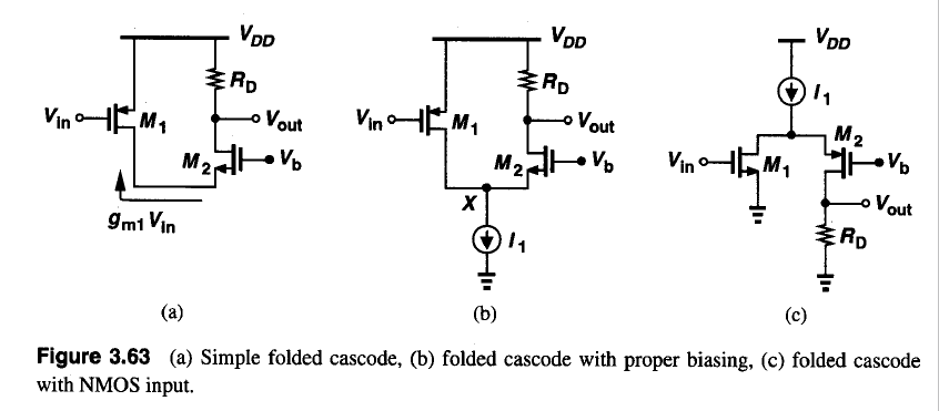
- 对于(b)
$$ \begin{aligned} I_{D2} &= I_1 - \frac{1}{2}k_p(V_{DD} - V_{in1} - |V_{tp}|)^2 \\ I_{D2} & \downarrow \ \Rightarrow I_{D2} = 0 \\ I_1 &= \frac{1}{2}k_p(V_{DD} - V_{in1} - |V_{tp}|)^2 \end{aligned} $$
$$ \begin{equation} V_{in1} = V_{DD} - |V_{tp}| -\sqrt{\frac{2I_{1}}{k_p}} \end{equation} $$
Folded Cascode With Current Source
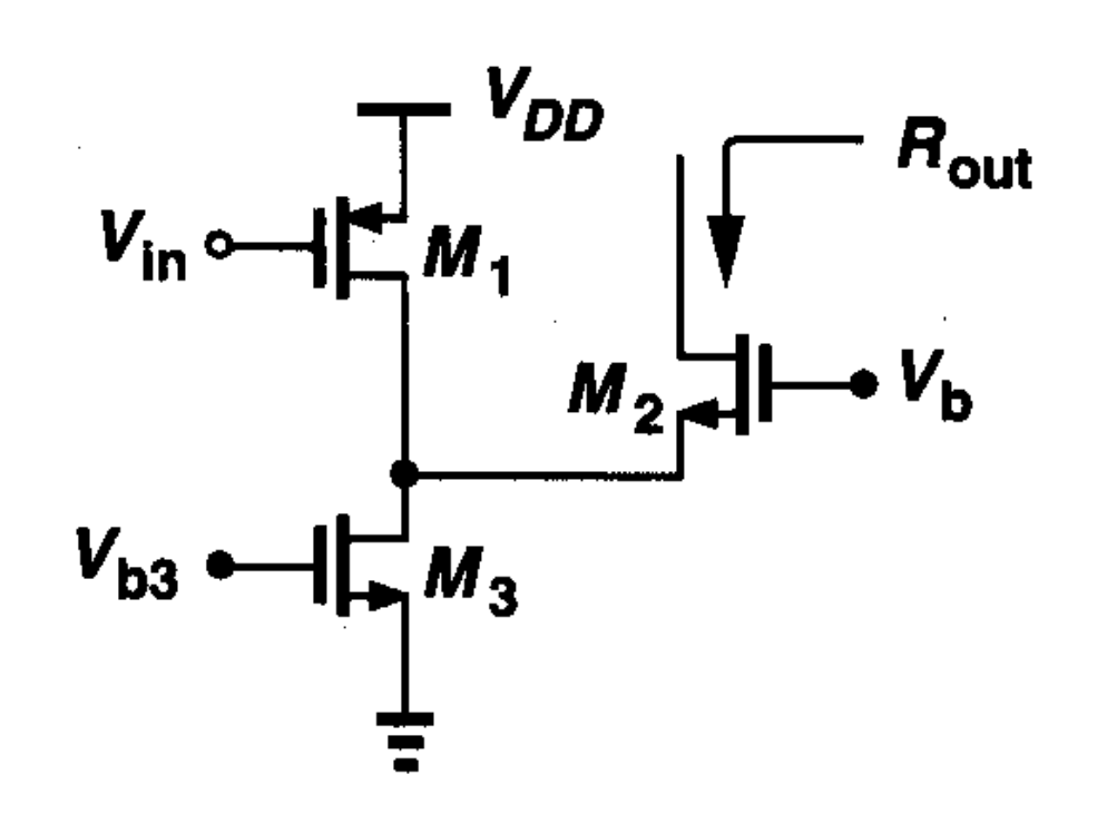
$$ \begin{equation} R_{out} = \big[ 1 + (g_{m2} + g_{mb2})r_{o2} \big] (r_{o1} || r_{o3}) + r_{o2} \end{equation} $$
附录
MOSFET的电阻
| 名称 | 输出电阻 | 反向输出电阻 | Triode Region Resistance |
|---|---|---|---|
| 符号 | $\dfrac{1}{g_m}$ 或 $r_{ds}$ | $r_o$ | $R_{on} = \dfrac{ V_{DS} }{ I_D }$ |
| 适用情况 | 考虑CLM | 进入Triode Region | |
| 不适用情况 | 高频电路 |
-
在饱和区,当MOSFET的输入电压足够高,使得MOSFET的通道完全打开,电流受限于外部电路阻抗而不是MOSFET本身。在这种情况下,MOSFET的漏-源电压和漏电流之间的关系可以近似为线性关系,类似于普通的电阻。
-
一般的, $r_o \gg \frac{1}{g_m}$
Body Effect
the voltage at the body terminal (which is usually connected to the source) affects the threshold voltage of the device. This occurs because of the depletion region that forms between the body and channel regions. When a voltage is applied to the body, it changes the width of this depletion region, which alters the effective thickness of the oxide layer between gate and channel.
$$ \begin{equation} \eta = \frac{g_m}{g_{mb}} =\dfrac{\partial V_{TH}}{\partial V_{in}} = \frac{\partial V_t}{\partial V_{SB}} \end{equation} $$
-
在考虑Body Effect时, $V_t$是一个随电流变化的参数(一般情况下变化很小,忽略不计)
-
$g_{mb}V_{bs}$
- 二极管的反向传输电阻对二极管电流的影响, 其中$g_{mb}$叫做反向跨导, 指栅-漏结电容在反向偏置下存储的电荷引起的漏极电流变化的比例,反映了MOSFET的输入特性。