组合电路
Multiplexer
数学表达式
$$ Z = \Sigma_{i=0}^{n-1} \ m_i D_i $$
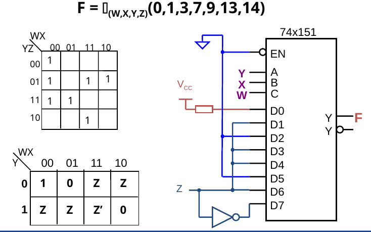
74x151 - 压缩卡诺图
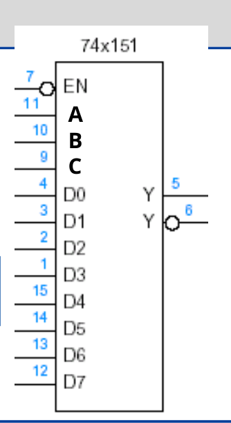
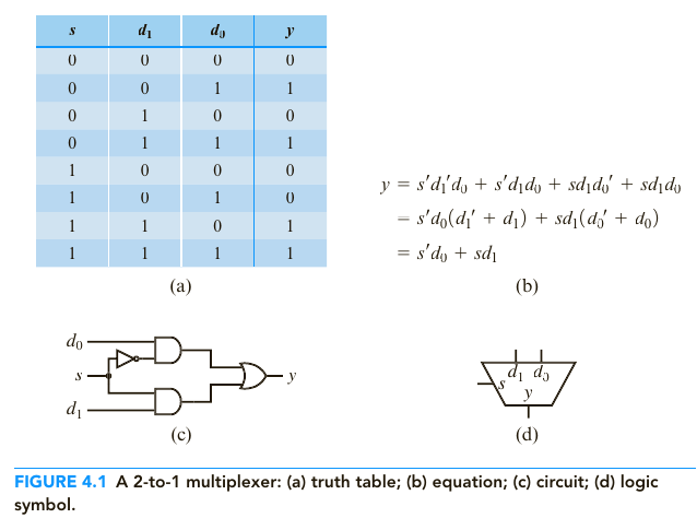
2-1 Multiplier
加法器
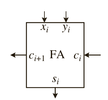
Full Adder
- 过程
- 真值表与实现效果
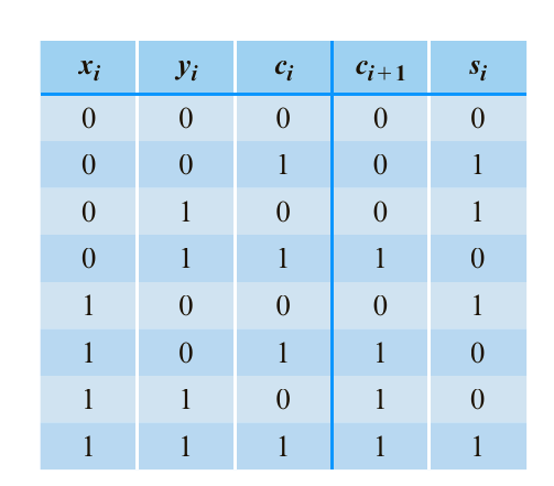
$$ x_i + y_i + c_i = s_i \\\ \\ 溢出到c_{i+1} $$
- 逻辑表达
$$ \begin{aligned} s_i &= SOP \\ c_{i+1} &= POC \\ s_i &= x_i \oplus y_i \oplus z_i \\ c_{i+1} &= x_iy_i + c_i(x_i \oplus y_i) \end{aligned} $$
- 电路
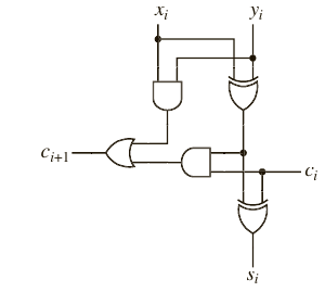
- 逻辑符号
- Verilog Code for a 1-bit FA
|
|
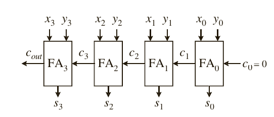
Ripple-Carry Adder (串位进行加法器)
- 定义
- 级联多个FA, 每一个FA都要等待上一位的输出,效率低下
- 通过 RCA实现4-bit adder
- Verilog
|
|
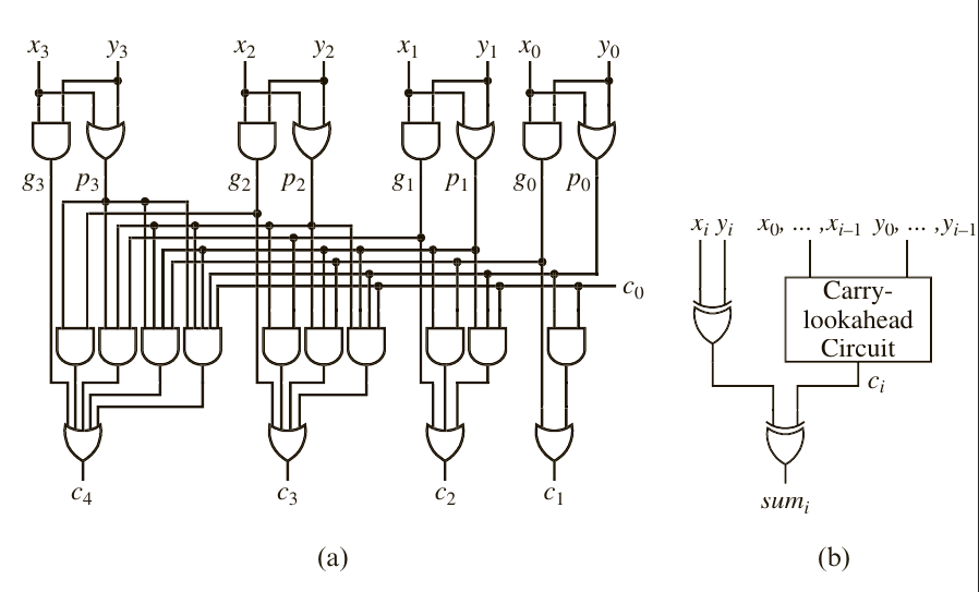
Carry-Lookahead Adder (进位预测加法器)
-
只适用于无符号数
-
前提与分析
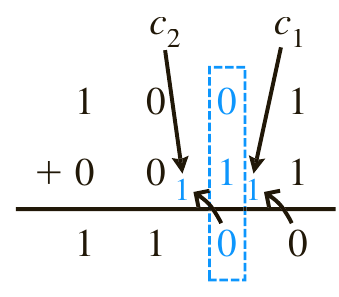
$$ \begin{aligned} c_{i+1} &= x_iy_i + (x_i + y_i)c_i \\\ \\ Let \ g_i &= x_iy_i \\ \ p_i &= x_i + y_i \\\ \\ c_1 &= g_0 + p_0c_0 \\ c_2 &= g_1 + p_1c_1 \\ &= g_1 + p_1(g_0 + p_0c_0) \\ &= g_1 + p_1g_0 + p_ip_0c_0 \\ c_3 &= g_2 + p_2g_1 + p_2p_1g_0 + p_2p_1p_0c_0 \\ c_4 &= g_3 + p_3g_2 + p_3p_2g_1 + p_3p_2p_1g_0 + p_3p_2p_1p_0c_0 \end{aligned} $$
- 电路
减法器 (无符号数)
输出
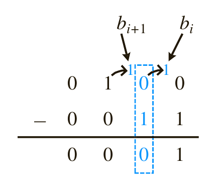
实现方式
$$ \begin{aligned} 被减数为B,减数为A \\ A-B &= A+(-B) \\ 通过补码,-B &= B’ + 1 \\ 因此, F &= A - B = A+ B’ +1 \end{aligned} $$
逻辑函数与其他参数
$$ \begin{aligned} d_i &= x_i \oplus y_i \oplus z_i \\ b_{i+1} &= x_i’b_i + x_i’y_i + y_ib_i \end{aligned} $$
加法和减法器的结合
原理 真值表 电路 逻辑符号
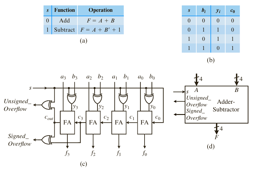
溢出的处理与公式
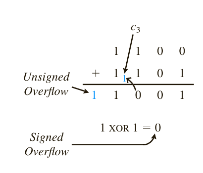
$$ \begin{aligned} 减法: Signed \ Overflow &= (A_n\cdot B_n’ \cdot F_n’) + (A_n’\cdot B_n\cdot F_n) \\ 加法: Signed \ Overflow &= (A_n’ \cdot B_n’ \cdot F_n) + (A_n\cdot B_n\cdot F_n’) \end{aligned} $$
Verilog实现代码
|
|
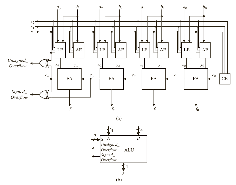
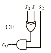
ALU
4位ALU电路和逻辑符号
操作表 真值表
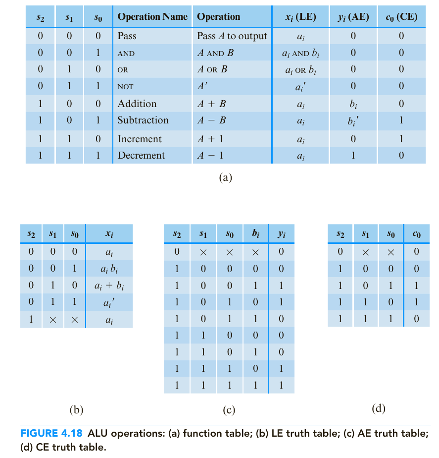
- 通过卡诺图化简(只考虑$s_2 = 0 \ or \ 1$, 这样就只有四个变量)
组成单元
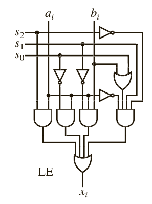
LE (Logic Extender)
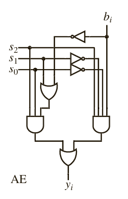
AE (Arithmatic Extender)
CE (Carry Extender)
Verilog代码
行为代码
|
|
数据流和结构代码
|
|
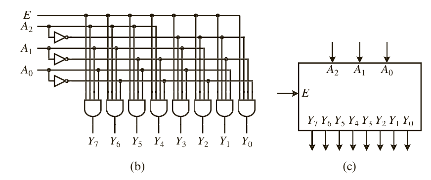
Decoder
电路和逻辑符号
Verilog
|
|
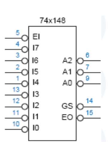
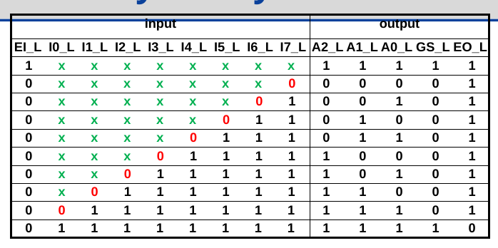
Encoder
74x148 Encoder
- 电路图
- 工作原理
Verilog
|
|
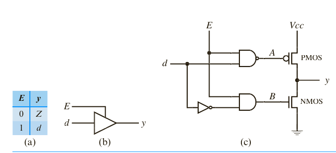
Tri-State Buffer
性质与作用
-
三种状态: 高电平、低电平、高阻态(等价于断路)
-
放大输入信号后输出
-
高阻态下不干扰其他电器工作
电路和逻辑符号
Verilog
|
|
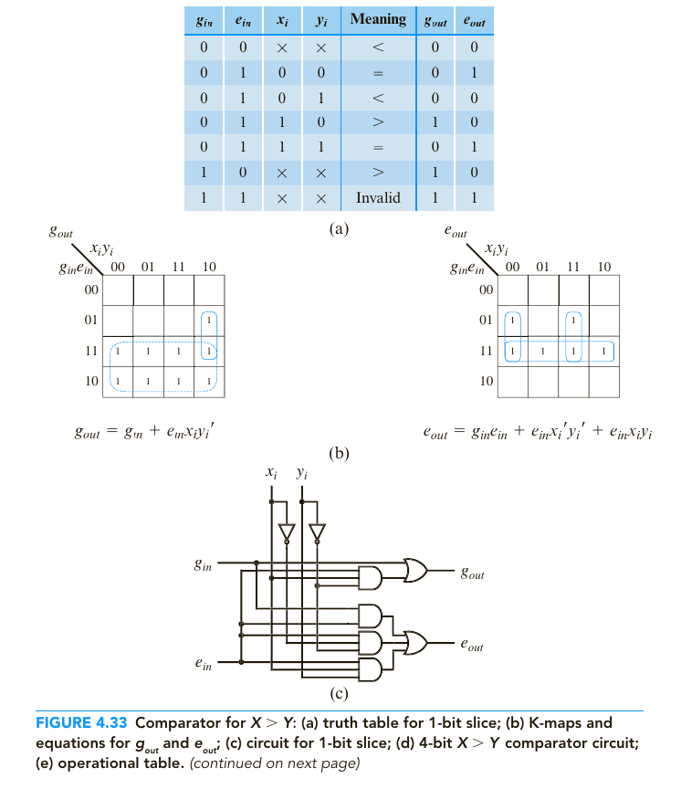
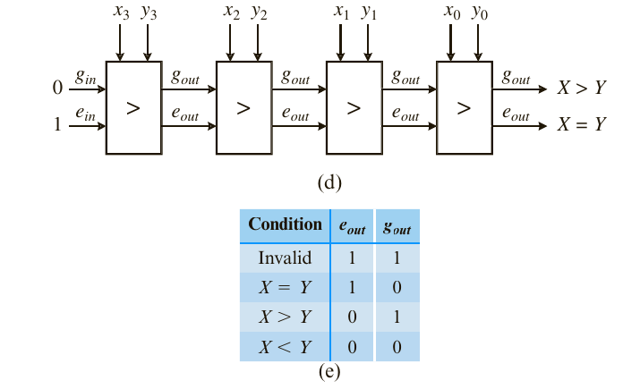
Comparator
常见的四位比较器
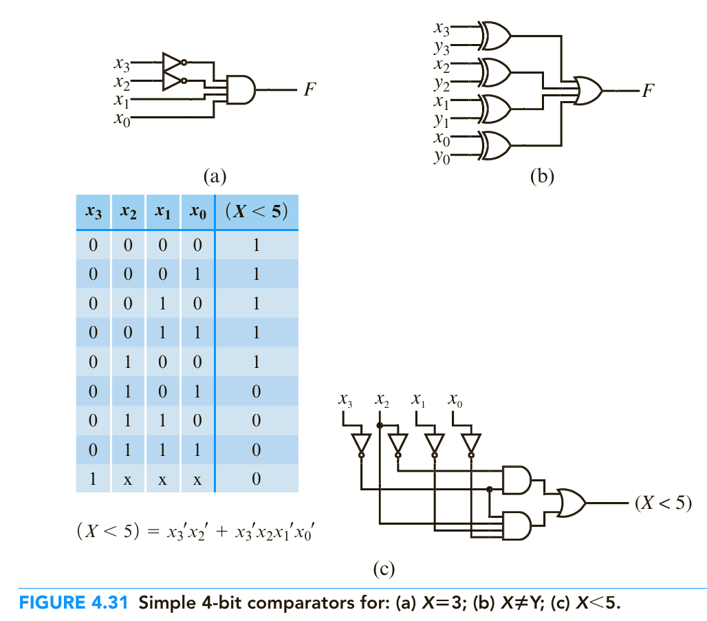
4-bit X > Y Comparator
- 设计
- Verilog (Behavioral Code)
|
|
Shifter
类型
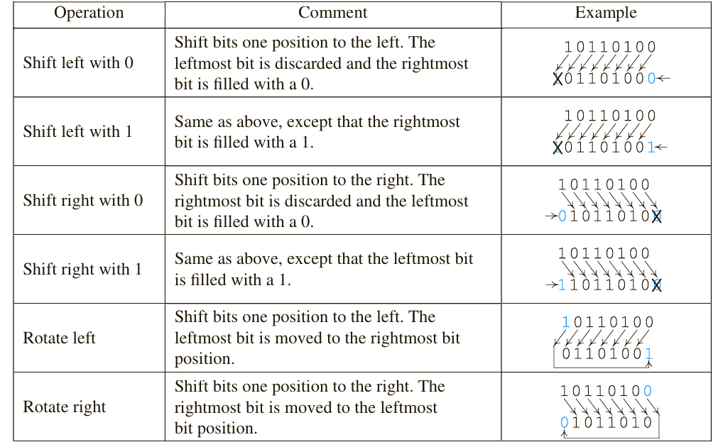
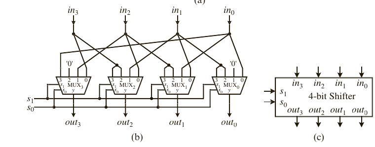
4-bit Shifter
Verilog
|
|
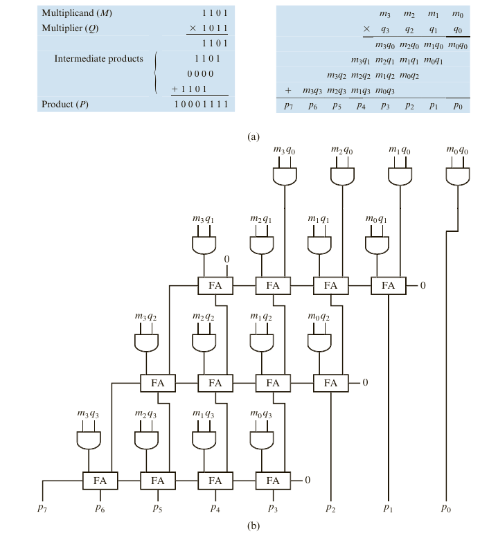
Multiplier
原理 电路图
Verilog
|
|
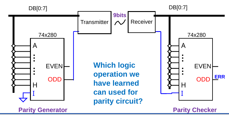
Parity Generator/Checker
电路
- 校验位
- 奇数为1. 偶数为0
Verilog
|
|
门电路
Fan
Fan-in (of a logic family)
The number of inputs that a gate can have in a particular logic family
Fan-out (of a logic family)
The number of outputs that a gate can have in a particular logic family
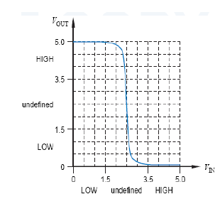
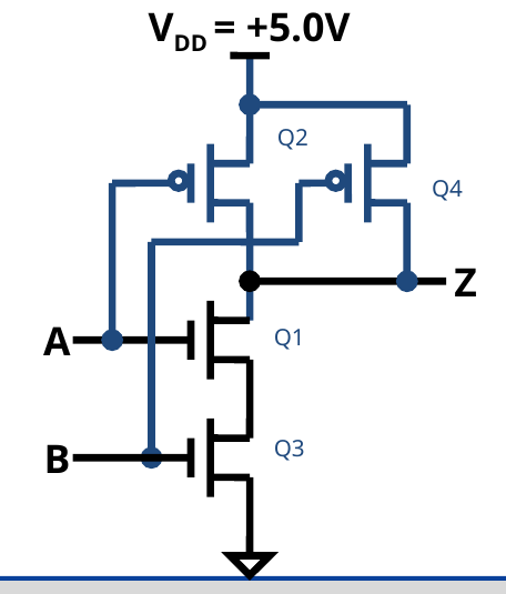
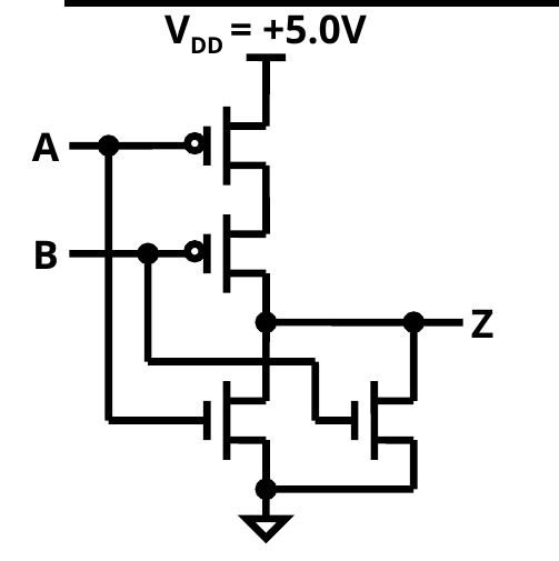
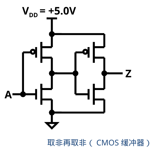
CMOS反相器
电路
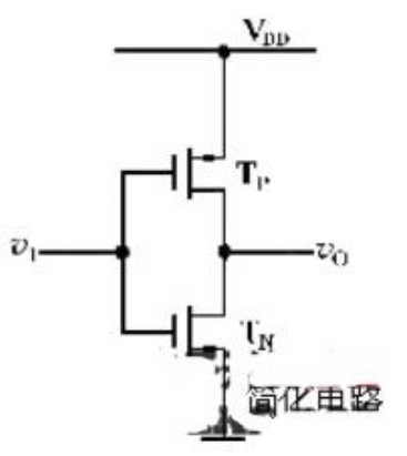
图像
-
低电位时,PMOS导通,NMOS截止
-
高电位时,PMOS截止,NMOS导通
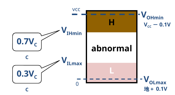
CMOS 逻辑系列电平规格
上/下拉电阻
- 上拉$p$电阻
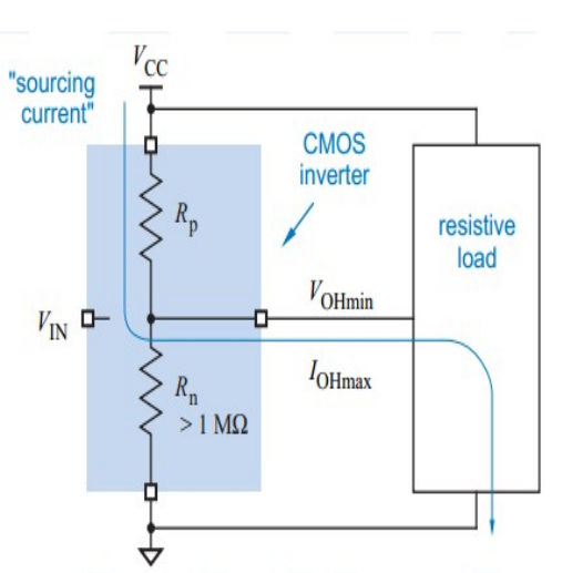
$$ 上拉电阻 \ R_{p(on)} = \frac{V_{CC} - V_{OHminT}}{|I_{OHmax}|} $$
- 下拉$p$电阻
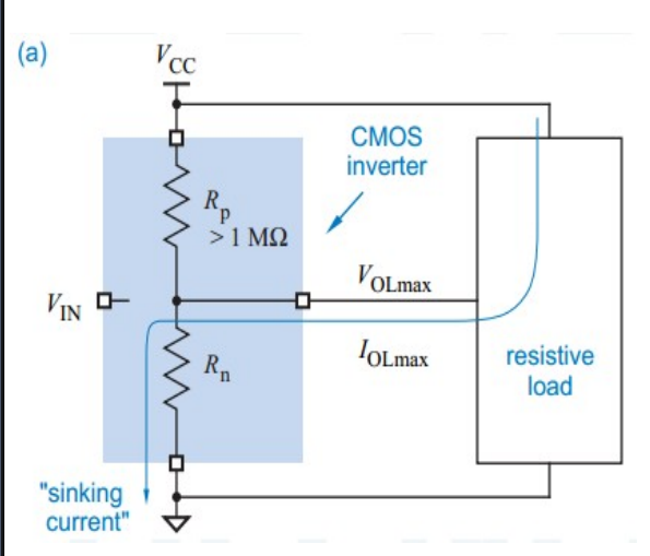
$$ R_{n(on)} = \frac{V_{OLmax}}{I_{OLmax}} $$
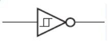
- Schmitt-trigger Inverter
-
当输入信号超过阈值时,输出信号会发生反转
-
具有高的噪声抑制能力和稳定性
与非门
- 最多6输入
或非门
- 最多4输入
非反相门
与或非门
附录
有源电路
- 有源电路是指包含电源或其他能够提供电能的元件的电路,例如电子管、晶体管、集成电路等