Bistable Element
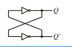
- 串联两个Inverter达到保持input和output都不变的效果
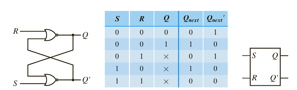
SR Latch (Set Reset) - SR 锁存器
与非门
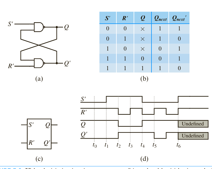
或非门
Gated SR Latch / S Latch With Enable (NAND)
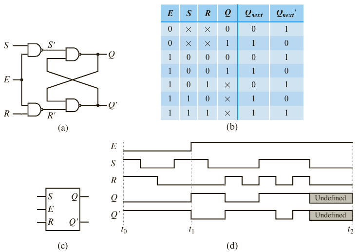
D Latch (NAND)
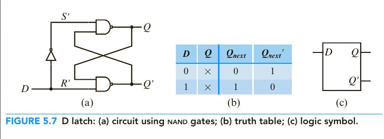
- 效果:输出端保持稳定
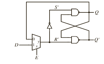
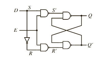
Gated D Latch
- 2 NAND
- 4 NAND
Verilog Code
|
|
总结
| NAND | NOR |
|---|---|
| 输入为$11$是不稳定的 | 输入为00是不稳定的 |
Clock Divider
|
|
D Flip-Flop
定义
当时钟输入端接收到一个时钟信号时,将数据输入端的状态存储下来,并在下一个时钟信号到来前保持不变
Behavioral Verilog
|
|
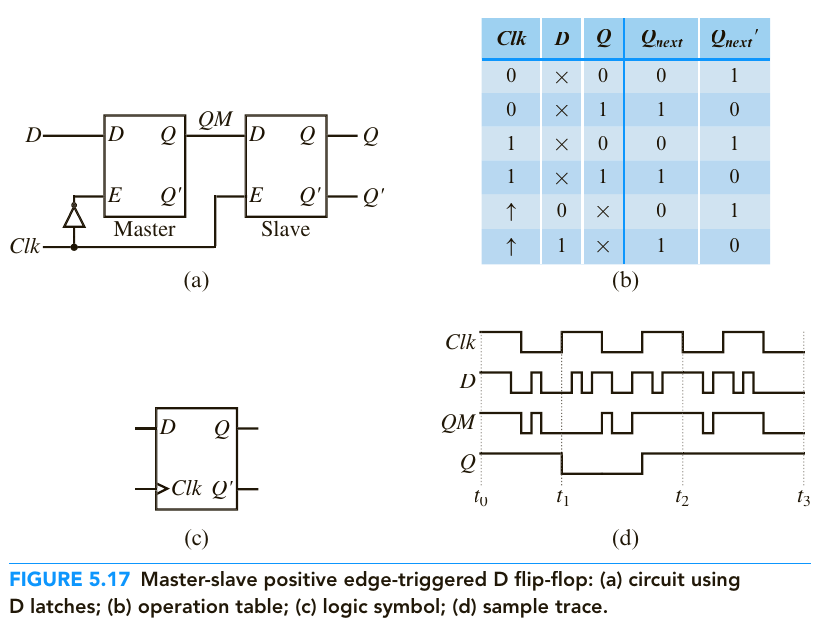
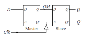
Master-slave positive edge-triggered D flip-flop
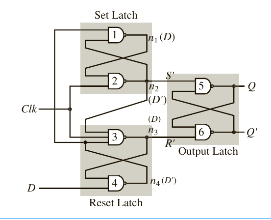
用SR-Latch 实现 D Flip-Flop
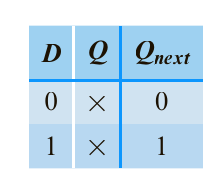
描述 - 状态图 方程 特征表
stateDiagram
Q=0 --> Q=1: D=1
Q=0 --> Q=0: D=0
Q=1 --> Q=0: D=0
Q=1 --> Q=1: D=1
$$ Q_{next} = D $$
master-slave negative edge-triggered D flip-flop
D flip-flop With Enable

Register File
定义
存储CPU中的通用寄存器
Register Verilog
|
|
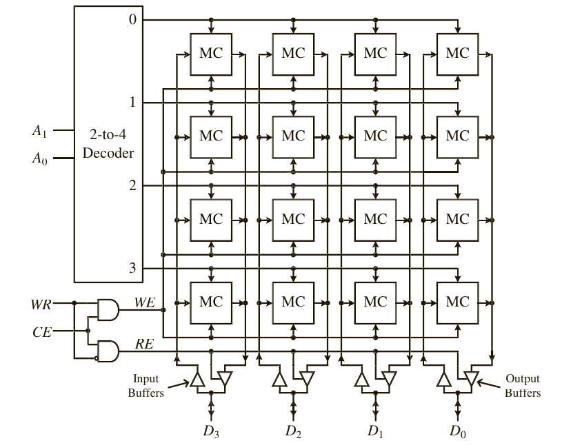
4 location x 8-bit Register File Circuit
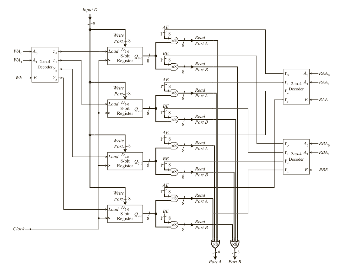
| WA | Write Address |
|---|---|
| WE | Write Enable |
| RAA | Read A Address |
| RAE | Read A Enable |
| RBA | Read B Address |
| RBE | Read B Enable |
Register File Verilog
|
|
4-bit bidirectional, parallel-in, parallel-out Register
74x194
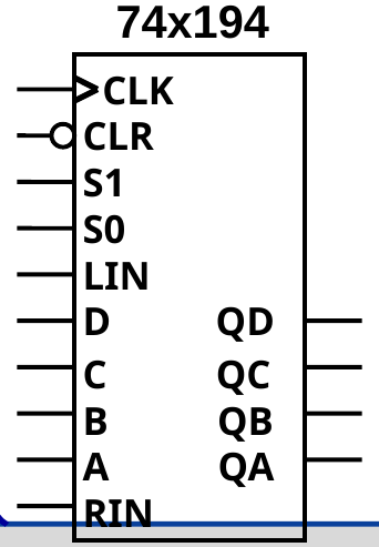
Function table
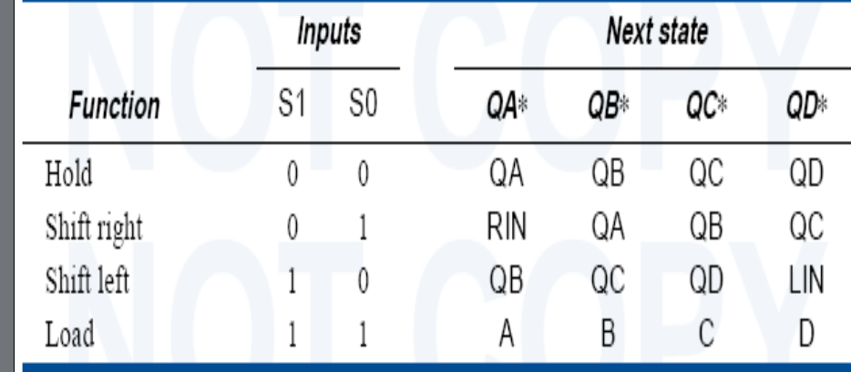
内存
ROM
逻辑符号 操作表
Verilog
|
|
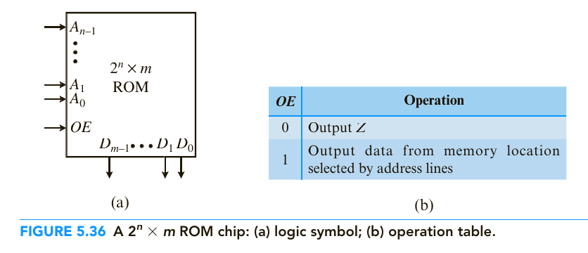
RAM
逻辑符号 操作表
$4\times 4$ RAM
经典RAM Verilog 代码
| CE | WR | EO |
|---|---|---|
| Chip Enable | Write | Enable Output |
|
|
$32\times 8$ RAM used in EC-2 Microprocessor
|
|
Shift Register
4-bit serial-to-parallel register
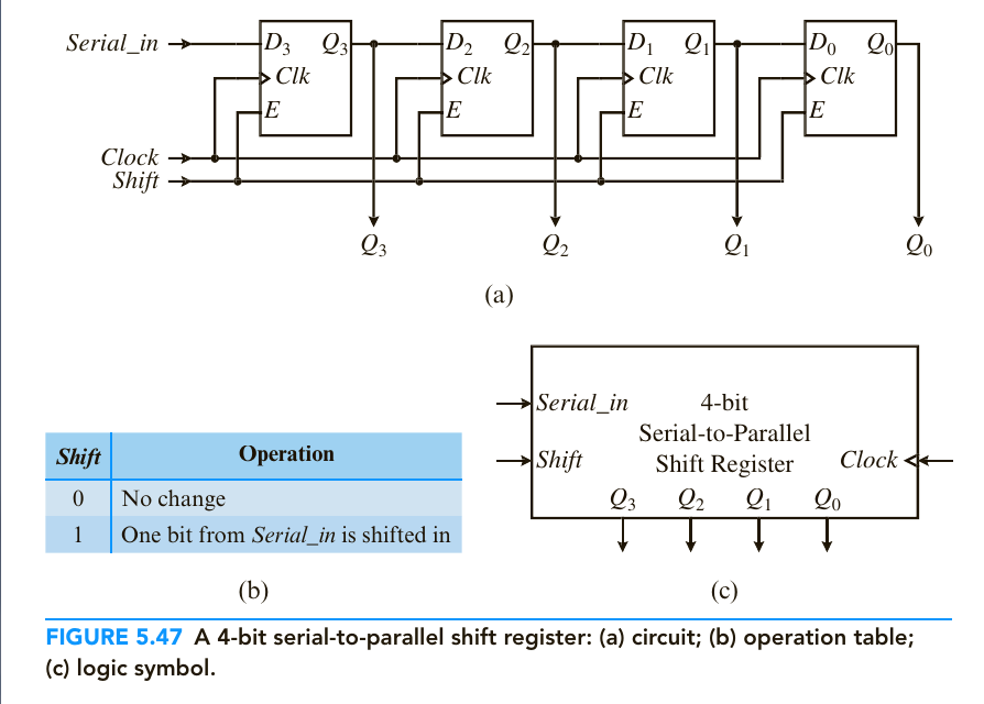
Right Shift Register
|
|
Counter
4-bit Binary Up Counter
Verilog
|
|
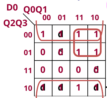
74x163 - 4-bit Binary Synchronous Counter
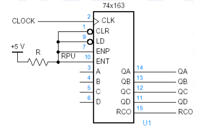
RCO (Reset Carry-Out)
- 复位同步输出引脚。当计数器达到最大计数值时,RCO引脚会输出一个脉冲信号,用于将其他电路中的计数器复位或同步。用于同步多个计数器的计数。
Shift-Register Counters
定义
将一个二进制数字序列存储在移位寄存器中,然后通过移位操作将其向左或向右移动,从而实现计数。当移位寄存器中的数字序列达到最大值时,计数器会重新开始计数。可以使用单个移位寄存器或多个级联的移位寄存器来实现不同的计数分辨率
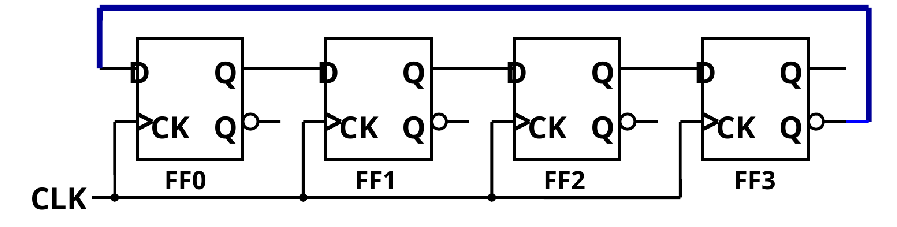
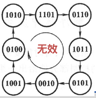
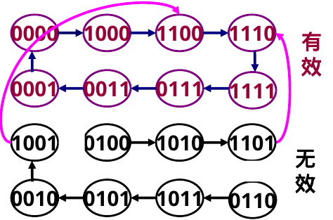
Ring Counters
电路
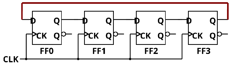
状态
- 主状态(有效状态)
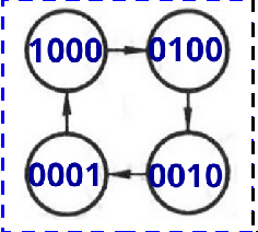
- 无效状态
Self-Correcting
Johnson Counter (扭环计数器)
电路
状态
- 有效状态
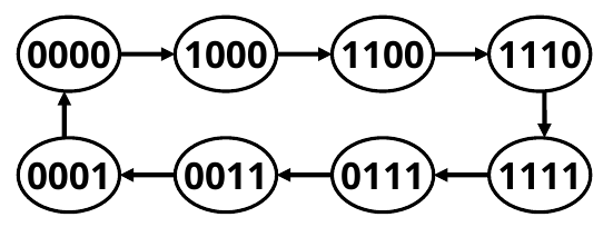
- 无效状态
Self-Correcting
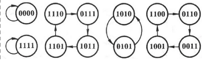
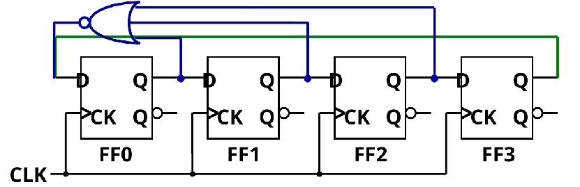
Linear Feedback Shift Register Counters (LFSR)
Serial Signal Generator
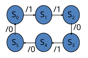
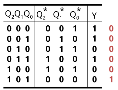
Example - Serial Signal Generator (110100)
Dff (D触发器)
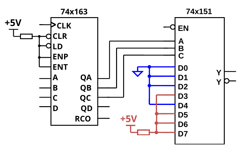
163 -> 151
Shift Register
Timing Analysis
Timing issue
- 时钟偏移、信号延迟、时序失配、时序噪声等
Hazards in Digital System
定义
Combinational Circuit 中出现的不期望的输出
Static hazard (glitch)
- Static 1 hazard
- the output changes from 1 to 0 and back to 1
- Static 0 hazard
- the output changes from 0 to 1 and back to 0
Dynamic hazard (bounce)
-
Dynamic 0 to 1 hazard: the output changes from 0 to 1 to 0 to 1
-
Dynamic 1 to 0 hazard: the output changes from 1 to 0 to 1 to 0
Synchronous & Asynchronous
-
Preset = Set, Clear = Reset
-
在时钟的上升/下降沿改变的信号叫做同步信号, 否则是异步信号