有MOSFET的放大器
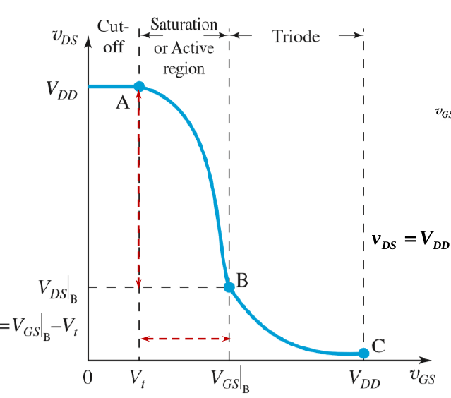
Voltage-Transfer Characteristics
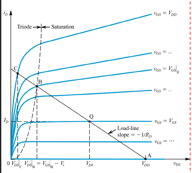
图示
公式
$$ \begin{gather} \begin{aligned} V_{DS} &= V_{DD} - i_DR_D \\ &= V_{DD} - \frac{1}{2}k_nV_{OV}^2R_D \end{aligned} \end{gather} $$
- 对于Active和Triode的临界点$\pmb B$
$$ \begin{gather} \begin{aligned} V_{DS}|B &= V{GS}|B -V_T \\ &= V{OV} \\ &= \frac{\sqrt{2k_n R_D V_{DD}+1}-1}{k_nR_D} \end{aligned} \end{gather} $$
$$ \begin{gather} \begin{aligned} V_{GS}|B &= V_t + V{DS}|B \\ &= V_t + \frac{\sqrt{2k_n R_D V{DD}+1}-1}{k_nR_D} \end{aligned} \end{gather} $$
偏压获得线性放大
- Q点: bias point/dc operating point/ quiescent point
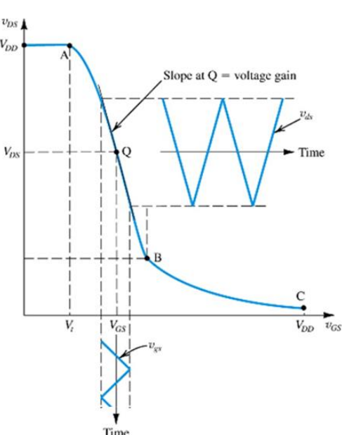
小信号电压增益
电流
$$ \begin{aligned} i_D &= I_D + i_d \\ &= \frac{K(V_{GS}+v_{GS}-V_T)^2}{2} \\ &= \frac{K(V_{GS}-V_T)^2}{2} + K(V_{GS}-V_T)v_{gs} + \frac{K}{2}v_{gs}^2 \\ &= dc + linear \ Gain + nonlinear \ distortion \\ \frac{1}{2}kv_{gs}^2 &\ll kv_{ov}v_{gs} \\ v_{gs} &\ll 2v_{ov} \\ &由于v_{gs}^2太小,直接\pmb{忽略第三项} \\\ i_D &= \frac{K(V_{GS}-V_T)^2}{2} + K(V_{GS}-V_T)v_{gs} \\ i_D &= I_D + i_d \\ i_d &= KV_{OV}v_{gs} \end{aligned} $$
电导
$$ \begin{aligned} g_m &= \frac{\partial i_d}{\partial v_{GS}}\Big|{v{gs} = V_{GS}} \\ &= \frac{d[\frac{1}{2}k_n(V_{GS}-V_t)^2]}{dv_{GS}}\Big|{v{gs} = V_{GS}} \\ &= \pmb{k_nV_{OV}} \\ \because I_D &= \frac{1}{2}k_nV_{OV}^2 \Longrightarrow V_{OV} = \frac{\sqrt{2I_D}}{\sqrt{k_n}} \\ \therefore g_n &= \sqrt{2k_nI_D} = \frac{2I_D}{V_{OV}} \end{aligned} $$
增益
$$ \begin{aligned} V_{DS} &= V_{DD} - i_DR_D \\ &= V_{DD} - (I_D + i_d)R_D \\ &= V_{DD} - I_DR_D -i_dR_D \\ A_v &= \frac{v_o}{v_i} = \frac{v_{ds}}{v_{gs}} = -g_mR_D \\ I_D &= \frac{1}{2}KV_{OV}^2 \Longrightarrow K = \frac{2I_D}{V_{OV}^2} \\ \therefore A_v &= -\frac{I_D R_D}{V_{OV}/2} = -g_m R_D \\ \end{aligned} $$
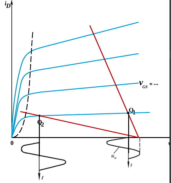
通过图像分析确定VTC
图像
Q on IVC ($V_{GS}$ is fixed)?
-
Point $Q_1$ is too close to $V_{DD}$, resulting in the positive peaks of the signal being clipped off which is called the circuit does not have sufficient “headroom”
-
Point $Q_2$ is too close to the boundary of the triode region, thus severely limiting the allowable negative signal swing of vds, resulting in a distorted output signal. In this situation the circuit does not have sufficient “legroom.”
Example
E.x.1
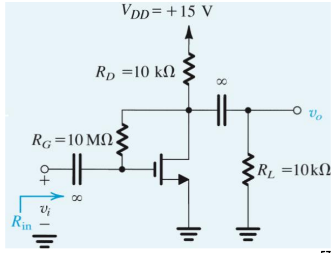
题目
$$ (1)V_t = 1.5V, k’n(W/L) = 0.25mA/V^2 \\\ \\ (2)V_A = 50V (晶体管的最大反向漏极电压) $$
问题
-
small-signal voltage gain
-
input resistance, the largest allowable input signal
解答
- 分析电路
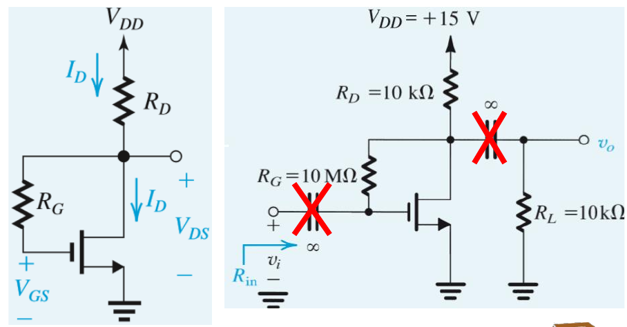
$$ DC不流过R_G \Longrightarrow V_{GS} = V_{DS} = V_{DD} - I_DR_D\\\ \\ I_D = \frac{1}{2} k_nV_{OV}^2 \\\ \\ \therefore I_D = 1.06(mA) , V_{GS} = V_{DS} = 4.4(V), V_{OV}= V_{GS} - V_t =2.9(V) \\\ \\ g_m = k_nV_{OV} =0.725(mA/V) $$
- 继续转换电路
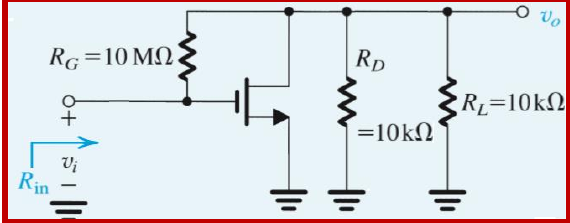
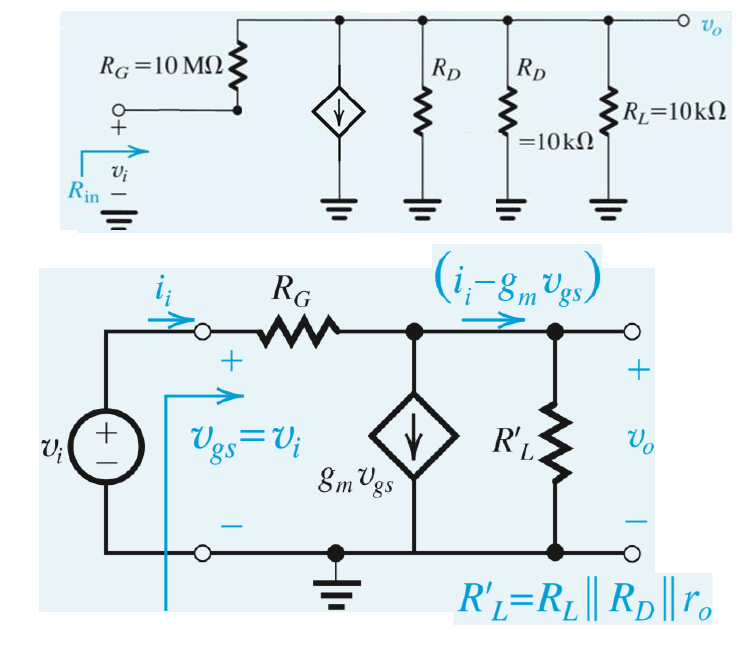
- 分析
$$ r_o =\frac{V_A}{I_D} = 47(k\Omega) \\\ \\ R’L = R_L || R_D || r_o = 4.52(k\Omega) \\\ \\ i_i = \frac{v{gs}-v_o}{R_G} \\\ \\ v_o = (i_i - g_mv_{gs}) R_L’ \\\ \\ (2) A_v = -g_m R_L’ \frac{1-(1/g_mR_G)}{1 + (R_L’ /R_G)} = -3.3(V/V) \\\ \\ V_{DS} \ge V_{OV} \\\ \\ V_{DS min} = V_{GS max} -V_t \\\ \\ V_{DS} - |A_v| v_{ip} = V_{GS} + V_{ip} -V_t \\\ \\ \because V_{GS } = V_{DS} \\\ \\ V_{iP max} = \frac{V_t}{|A_v| + 1} $$
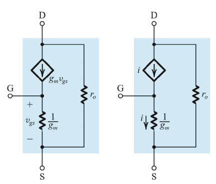
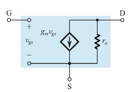
Model
T Equivalent-Circuit Model
- 在电路中加入第二个MOSFET (不影响电路特性)
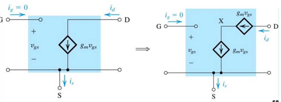
-
连接$X$和$G$,根据$KCL$方程,没有电流流入G
-
将原MOSFET等效为一个$\frac{1}{g_m}$的电阻
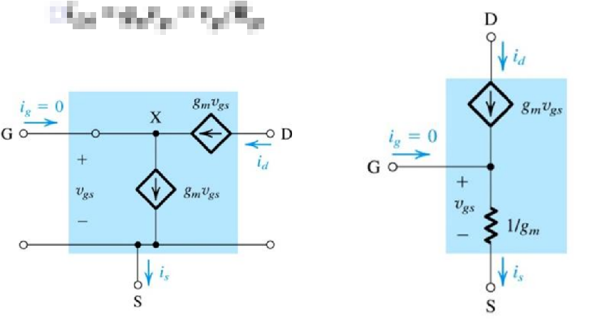
- 最终电路(加上内阻$r_0$)
Hybrid-$\pi$ Model
如何选择模型
-
Source端的电压是固定的 $\Longrightarrow \ \pi$ Model
-
Source端接电阻等 $\Longrightarrow$ T Model
Basic MOSFET Amplifier Configurations
The Common-Source Amplifier with a Source Resistance
等效图示
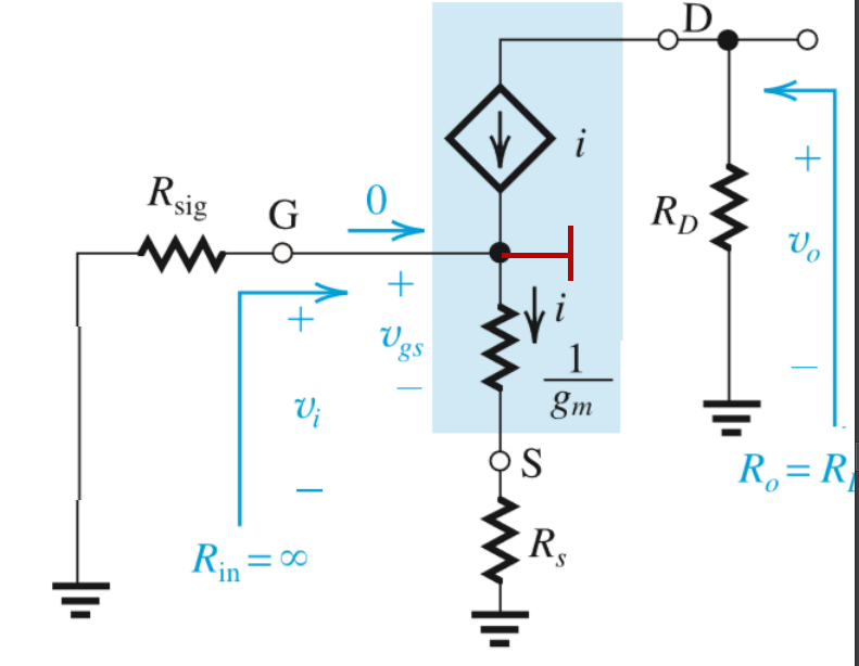
分析
$$ R_{in} = \infin \\\ \\ R_{out} = R_D $$
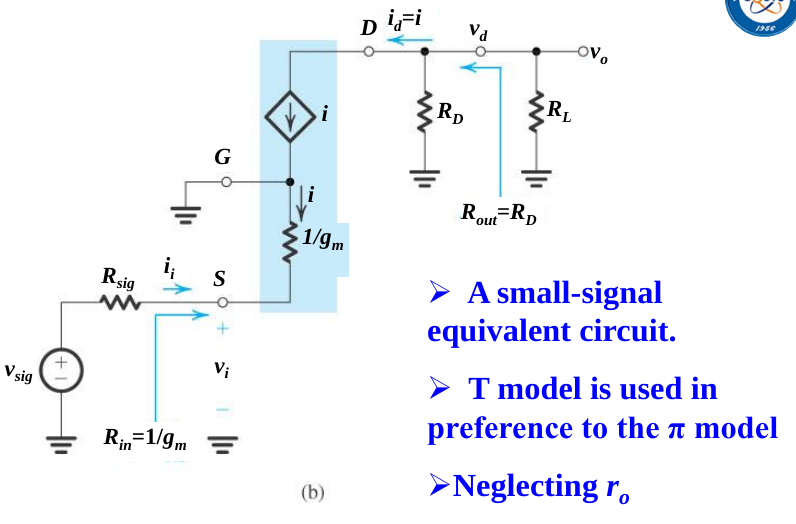
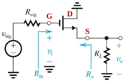
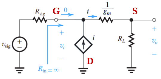
The Common-Gate (CG) Amplifier
电路
- 原电路
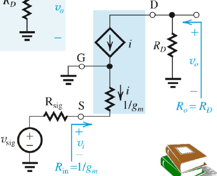
- 变换后
分析
$$ R_{in} = \frac{1}{g_m} \\\ \\ R_{out} = R_D \\\ \\ A_{vo} = \frac{v_o}{v_{i}} = \frac{-iR_D}{-i\frac{1}{g_m}} = g_mR_D \\\ \\ G_v = \frac{v_o}{v_{sig}} = \frac{-(R_L || R_D)}{-(R_{sig} + \frac{1}{g_m})i}= \frac{g_m R_L || R_D}{1 + g_m R_{sig}} $$
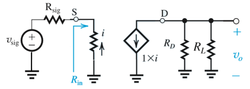
The Common-Drain Amplifier (Source Follower)
电路
- 原始
- 变换后
分析
- 因为都接地,所以很多电压都相等
$$ R_{in} = \infin \\\ \\ V_o = g_m V_{gs}R_L = iR_L \\\ \\ A_{v} = \frac{iR_L}{i(R_L + \frac{1}{g_m})} \approx 1 \\\ \\ G_v = \frac{R_L}{R_L + \frac{1}{g_m}} \approx 1 \\\ \\ R_{out} = \frac{1}{g_m} \\\ \\ 区分Out和Load $$
比较
Biasing by Fixing $V_{GS}$
原因
$$ I = \frac{1}{2}\mu_nC_{OX} \frac{W}{L} (V_{GS} - V_t)^2 $$
-
$\mu_n$和$V_t$易受到温度影响
-
$V_t,\frac{W}{L},C_{OX}$即使在相同尺寸和型号的设备中变化也很大
Degeneration Resistance
电路
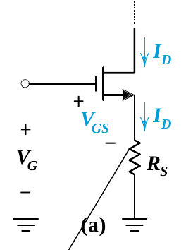
分析
$$ V_G = V_{GS} + I_DR_S (V_G \ is \ fixed)\\\ \\ I_D \uparrow \longrightarrow V_{GS} \downarrow \longrightarrow I_D \downarrow $$
Discrete-Circuit MOS Amplifiers
Common-Source Amplifier (反相放大器)
电路图
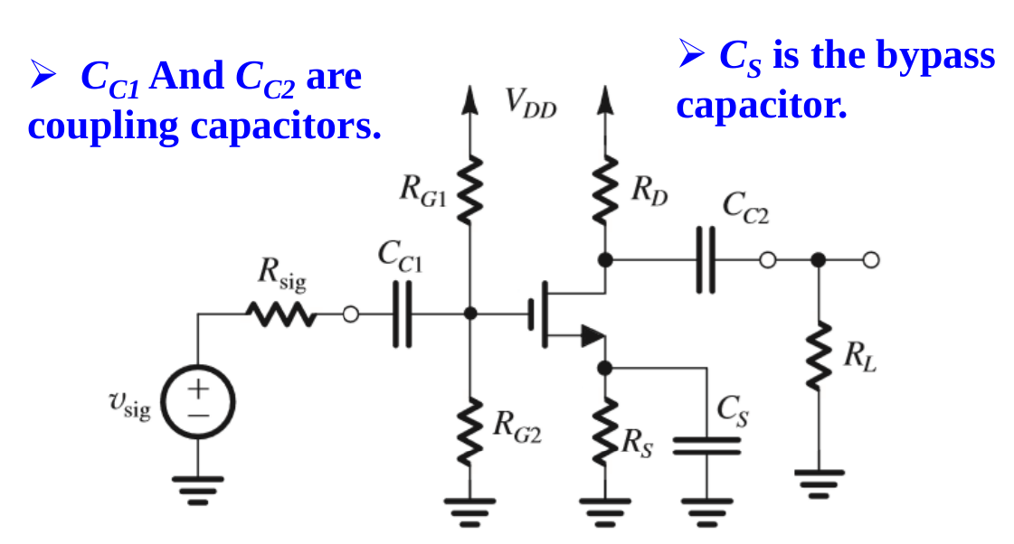
分析
- Coupling Capacitor
- 通交流,阻直流
- Bypass Capacitor
- 减少噪声
- 其他
$$ R_{in} = R_{G1} || R_{G2} \\\ \\ R_{o} = R_D || C_{C2} \approx R_D $$
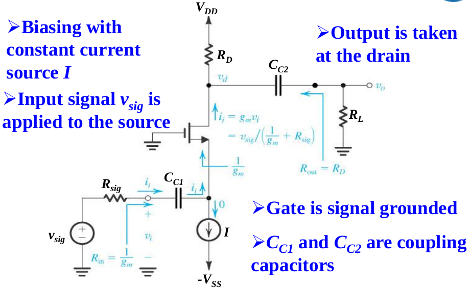
Common-Gate Amplifier
电路图
等效电路