IC Biasing
simple MOS constant-current source
电路
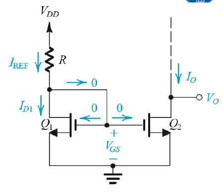
分析
$$ \begin{aligned} I_{D1} &= \frac{1}{2} k_{n1}’(\frac{W}{L})1 (V{GS} - V_{tn})^2 \\ &= I_{ref} \\ &= \frac{V_{DD} - V_{GS}}{R} \\ I_{D2} &= \frac{1}{2} k_{n2}’(\frac{W}{L})2 (V{GS} - V_{tn})^2 \\ \therefore \frac{I_{D1}}{I_{D2}} &= \frac{I_{ref}}{I_O} = \frac{(W/L)_1}{(W/L)_2} \\ \end{aligned} $$
MOS Current-Steering Circuit
电路
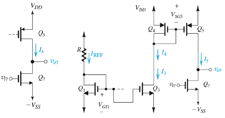
分析
$$ \begin{aligned} (1) &I_{1,2,3} \\ I_{D1} &= I_{REF} \\ V_{GS1} &= V_{GS2} = V_{GS3} = V_{GS} \\ \therefore \frac{I_{D1}}{I_{D2}} &= \frac{(W/L)2}{(W/L)1} \\ \therefore I{D2} &= I{REF} \frac{(W/L)2}{(W/L)1} \\ I{D3} &= I{REF} \frac{(W/L)_3}{(W/L)1} \\\ \\ (2) & I{4,5} \\ I_5 &= \frac{(W/L)_5}{(W/L)_4} I_4 \\ \end{aligned} $$
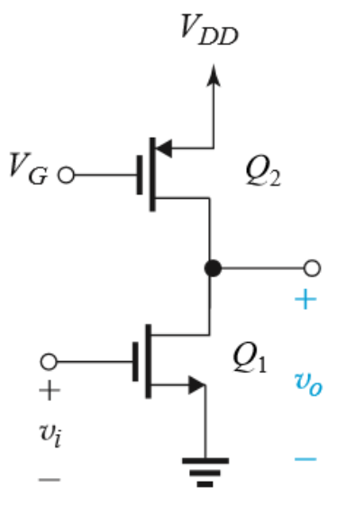
The Basic Gain Cell
定义(如图)
- Common Source + 偏置电流 I
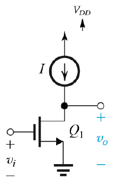
分析
电流
$$ 直流偏置点: I_D = I $$
电路转换
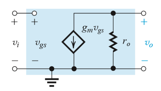
分析
$$ \begin{aligned} R_{in} &= \infin \\ R_o &= r_o \\ A_{vo} &= -g_mr_o \end{aligned} $$
电流源负载的输出阻抗效应
电路变换(CMOS)
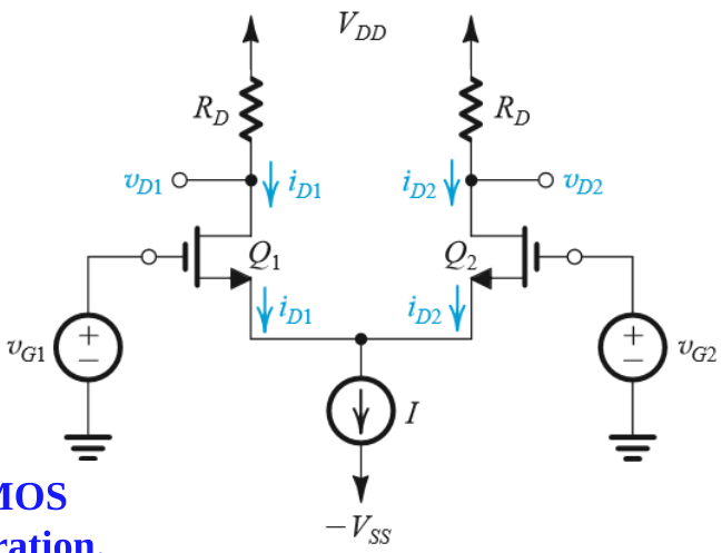
The MOS Differential Pair
Basic Configuration
图示
-
$V_{G1} - V_{T1} = V_{in1}$
-
$V_{G2} - V_{T2} = V_{in2}$
-
$V_{D1} = V_{out1}$
-
$V_{D2} = V_{out2}$
分析
- 增益
$$ \begin{aligned} V_{in1} - V_{in2} &= V_{GS1} - V_{GS2} \\ &= \sqrt{\frac{2I_{D1}}{k_n}} - \sqrt{\frac{2I_{D2}}{k_n}} \\ (V_{in1} - V_{in2})^2 &= \frac{2}{k_n}(I - 2\sqrt{I_{D1} I_{D2}}) \\ \because 4I_{D1}{I_{D2}} &= (I_{D1} + I_{D2})^2 - (I_{D1} - I_{D2})^2 \\ &= I^2 - (I_{D1} - I_{D2})^2 \\ \therefore (I_{D1} - I_{D2})^2 &= I^2 -4I_{D1}I_{D2} \\ &= -\frac{1}{4} k_n^2 (V_{in1} - V_{in2})^4 + I k_n(V_{in1} - V_{in2})^2 \\ \therefore I_{D1} - I_{D2} &= \frac{1}{2}k_n (V_{in1}- V_{in2}) \sqrt{\frac{4I}{k_n} - (V_{in1} -V_{in2})^2} \\ \frac{\partial \Delta I_D}{\partial \Delta V_{in}} &= \frac{1}{2}k_n \frac{\frac{4I}{k_n} - 2\Delta V_{in}^2}{\sqrt{\frac{4I}{k_n} - \Delta V_{in}^2} } \\ 当V_{in1} &= V_{in2} 时 \\ \frac{\partial \Delta I_D}{\partial \Delta V_{in}} &= \sqrt{k_n I} \\ \therefore |A_v| &= \frac{v_o}{v_i} \\ &= \sqrt{k_n I} R_D \end{aligned} $$
- 矛盾
-
在上述分析中,当$\Delta V_{in}$使得$\Delta I_D= 0$时,矛盾就出现了:
-
不同的$V_{in}$产生了相同的$I_D$
-
这是因为$\Delta I$和$\Delta V_{in}$的关系是在$M_1$和$M_2$都开启的条件下产生的
-
经过计算得知满足条件的$\Delta V_{in}$ 使得$M_2$ off, 故矛盾解决
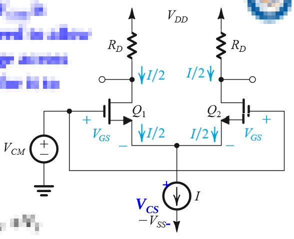
Common-Mode Input Voltage
电路
-
$Q_1 = M_1$
-
$Q_2 = M_2$
-
电流源是$M_3$
分析
$$ \begin{aligned} V_{G1} &= V_{G2} = V_{CM} \\ \frac{I}{2} &= \frac{1}{2} k_n V_{OV}^2 \\ V_{OV} &= \sqrt{\frac{I}{k_n}} (不变) \\ V_{D1} &= V_{D2} = V_{DD} -\frac{I}{2} R_D \\\ \\ V_{DS} &\ge V_{GS} -V_t \\ V_{D} &\ge V_G - V_t \\ V_{DD} - \frac{I}{2}R_D &\ge V_G - V_t \\ V_{CM} = V_{G} &\le V_{DD} -\frac{I}{2}R_D + V_t \\ \therefore V_{CMmax} &= V_{DD} -\frac{I}{2}R_D + V_t \\\ \\ V_{GS} &= V_{OV} + V_t \\ V_{CM} - V_S &= V_{OV} + V_t \\ V_{CM} - (V_{CS} + (-V_{SS})) &= V_{OV} + V_t \\ V_{CM} &= V_{CS} - V_{SS} + V_t + V_{OV} \\ V_{CM min} &= V_{CS \ min} -V_{SS} + V_t +V_{OV} \\\ \\ A_v &= \frac{V_{out}}{V_{in,CM}} \\ &= - \frac{R_D / 2}{1/(2g_m) + R_{SS}} \end{aligned} $$
电压关系
伏安特性曲线
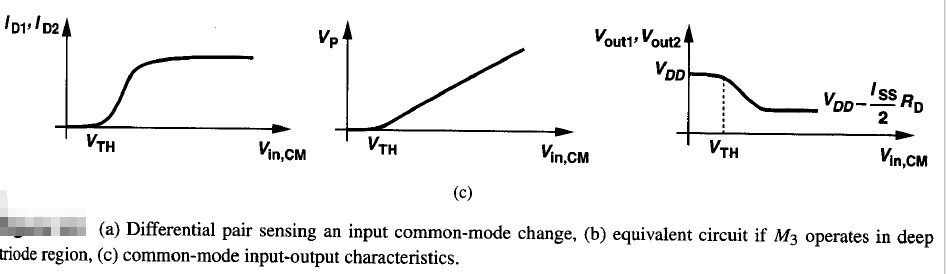
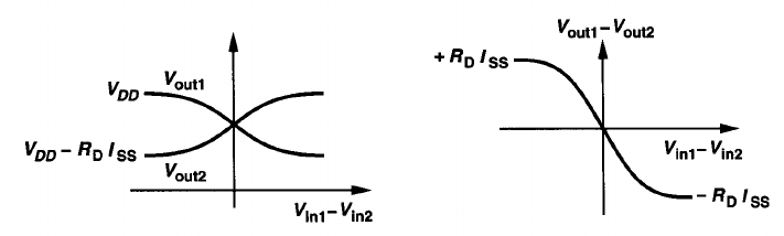
结论
-
Common-mode input voltage
-
Current I divides equally between two transistors
-
The difference between two drains is zero
-
The differential pair rejects the common-mode input signals
Differential Input Voltage
电路
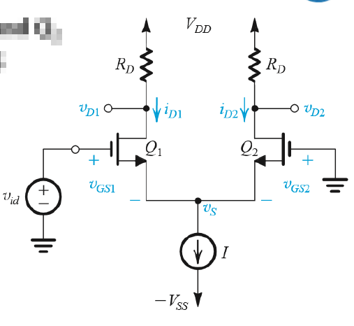
分析
$$ \begin{aligned} When \ i_{D1} &= I,V_S = -V_t \\ I&= \frac{1}{2}k_n(V_{GS1} -V_t)^2 \\ \therefore V_{GS1} &= V_t +V_{OV} \\ &= V_t +\sqrt 2 V_{OV \ 0.5I} \\ V_{id} - V_s &= V_t + \sqrt 2 V_{OV \ 0.5I} \\ V_{id} &= \sqrt{2} V_{OV \ 0.5I} \\\ \\ \therefore -\sqrt 2 V_{OV \ 0.5I} &\le v_{id} \le \sqrt 2 V_{OV \ 0.5V} \\ (V_{OV \ 0.5I} &= \sqrt{\frac{I}{k_n}}) \end{aligned} $$
结论
- The differential pair responds to a difference-mode
The Current-Mirror-Loaded MOS Differential Pair
电路
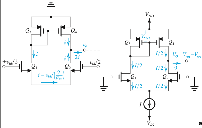
- $Q_3$和$Q_4$是构成了镜像电流源
分析
$$ \begin{aligned}
\end{aligned} $$
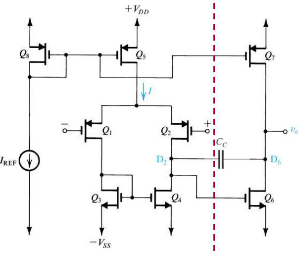
Two-Stage CMOS Op-Amp Configuration
Common-Mode Rejection
电路
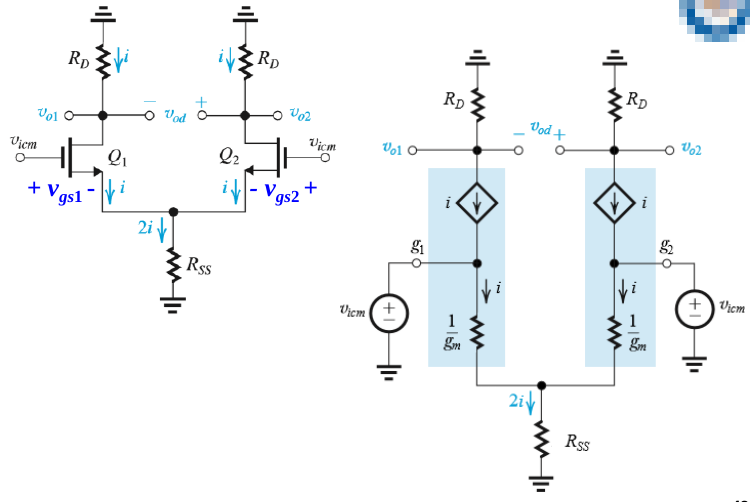
- $R_{SS}$ 是另一个MOSFET被等效后的源内阻$r_0$
分析
$$ \begin{aligned} (1) &对半电路分析 \\ V_{icm} &= i(2R_{SS} + \frac{1}{g_m}) \\ i &= \frac{v_{icm}}{2R_{SS} + \frac{1}{g_m}} \\ v_{o1} &= v_{o2} \\ & = -\frac{v_{icm}}{2R_{SS} + \frac{1}{g_m}} R_D \\ &\approx - \frac{v_{icm} R_D}{2R_{SS}} \\ v_{od} &= v_{o1} - v_{o2} \approx 0 \\ \therefore A_d &\approx - \frac{R_D}{2R_{SS}} \\\ \\ (2) 对&整个电路 \\ A_{CM} &= 0 \ (一正一负) \\ CMRR &= \frac{|A_d|}{|A_{cm}|} \\ &= \infin \end{aligned} $$
Large-Signal Operation
电路
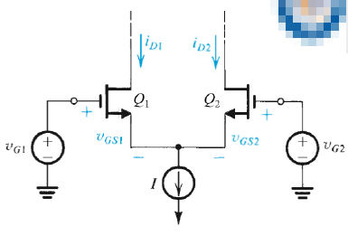
假设
-
不考虑CLM
-
工作在饱和区
-
Load Imdependence
分析
$$ \begin{aligned} i_{D1} &= \frac{1}{2}k_n(V_{GS1} -V_t)^2 \\ i_{D2} &= \frac{1}{2}k_n(V_{GS2} -V_t)^2 \\ V_{G1} - V_{G2} &= V_{id} = V_{GS1} - V_{GS2} \\\ \\ \sqrt{i_{D1}} -\sqrt{i_{D2}} &= \sqrt{\frac{1}{2} k_n} \ v_{id} \\ i_{D1} + i_{D2} &= I \\ 解得: i_{D1} &= \frac{I}{2} + \Big( \frac{I}{V_{OV0.5I}}\Big) \Big( \frac{v_{id}}{2} \Big) \sqrt{1 - \Big(\frac{v_{id}/2}{V_{OV 0.5I}}\Big)^2} \\ i_{D2} &= \frac{I}{2} - \Big( \frac{I}{V_{OV0.5I}}\Big) \Big( \frac{v_{id}}{2} \Big) \sqrt{1 - \Big(\frac{v_{id}/2}{V_{OV 0.5I}}\Big)^2} \\\ \\ \because \frac{v_{id}}{2} &\ll V_{OV 0.5I} \\ \therefore i_{D1} &\approx \frac{I}{2} + \Big( \frac{I}{V_{OV0.5I}}\Big) \Big( \frac{v_{id}}{2} \Big) \\ i_{D2} &\approx \frac{I}{2} - \Big( \frac{I}{V_{OV0.5I}}\Big) \Big( \frac{v_{id}}{2} \Big) \\ i_d &\approx \Big( \frac{I}{V_{OV0.5I}}\Big) \Big( \frac{v_{id}}{2} \Big) \\ g_m &= \frac{I}{V_{OV}} \ \ (I_D = \frac{I}{2}) \end{aligned} $$
Small-Signal Operation
Ex.
- 题目
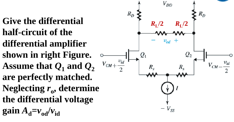
- 分析
- 因为对称, 把电路等效后差分成两个相同的电路
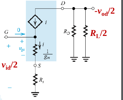
- 得到
$$ \begin{aligned} A_v &= \frac{R_D || (R_L/2)}{\frac{1}{g_m} + R_S} \end{aligned} $$
Appendix
直流偏置点
放大电路中交流信号的幅度变化围绕着一个直流电平进行,这个直流电平就是所谓的偏置点。在放大器中,通过设置适当的偏置点可以使得输出信号能够在不失真的情况下尽可能地接近于输入信号。