Layers in TSMC65nm
Metal Structure
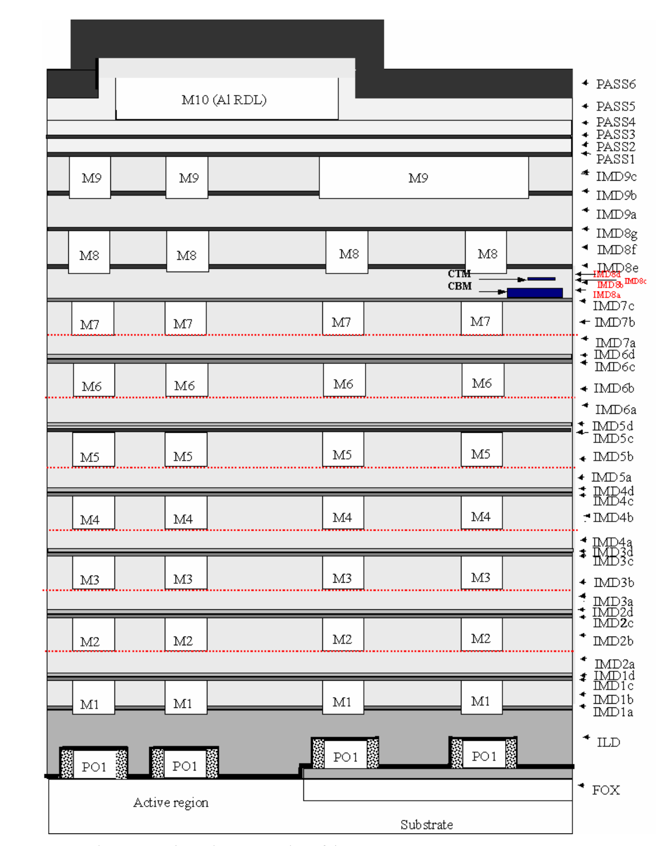
Purpose
| Purpose | 解释 |
|---|---|
| Ivs | 模拟芯片当前区域的当前消耗 |
| Pin | 分析引脚处的电压 |
| drw(drawing) | 绘制布局的物理层 |
| dm | 两个布图形状之间的最小距离 |
| BSW | BackSide Windowing |
| BSD | Backside Deposition |
Landscape
UI
| Category | Concept |
|---|---|
| AV | ALL Visable |
| NV | None Visable |
| AS | All Select |
| NS | None Select |
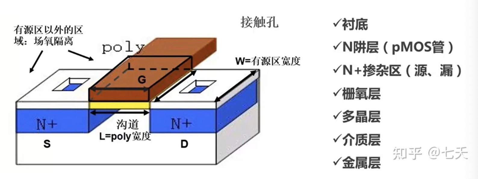
版图图层和物理图层的关系
| Category | Concept |
|---|---|
| PMOS | 必须画一个NWell |
| $N^+/ P^+$ | Active + n/p select (选择性参杂) |
| Gate-Oxide | 不显示 |
| Poly | 在Gate-Oxid上方, 在有源区上方的Poly才是栅极 |
| 介质层(Contact) | 金属层通过contact和晶体管连接才形成相应的极 |
| Metal | 与Source、GND连接的线 |
Components in TSMC65nm
Resistance
| Category | Concept |
|---|---|
| rm | 标准电阻 |
| rm…a | 用于高密度互连的电阻 |
| rm…z | 大电阻 |
Passive Components
On-Chip Capacitor
Introduction
It stores energy in electric field
| 名称 | 概念 |
|---|---|
| A | Overlapping Area |
| d | Separation |
| electric constant | $\varepsilon_0 = 8.854 \times 106{-12} F m^{-1}$ |
| dielectric constant | $\varepsilon_r$ |
$$ \begin{gather} \begin{aligned} C &= \varepsilon_0 \varepsilon_r \frac{ A }{ d } \end{aligned} \end{gather} $$
Category
MiM (Metal-Insulator-Metal)
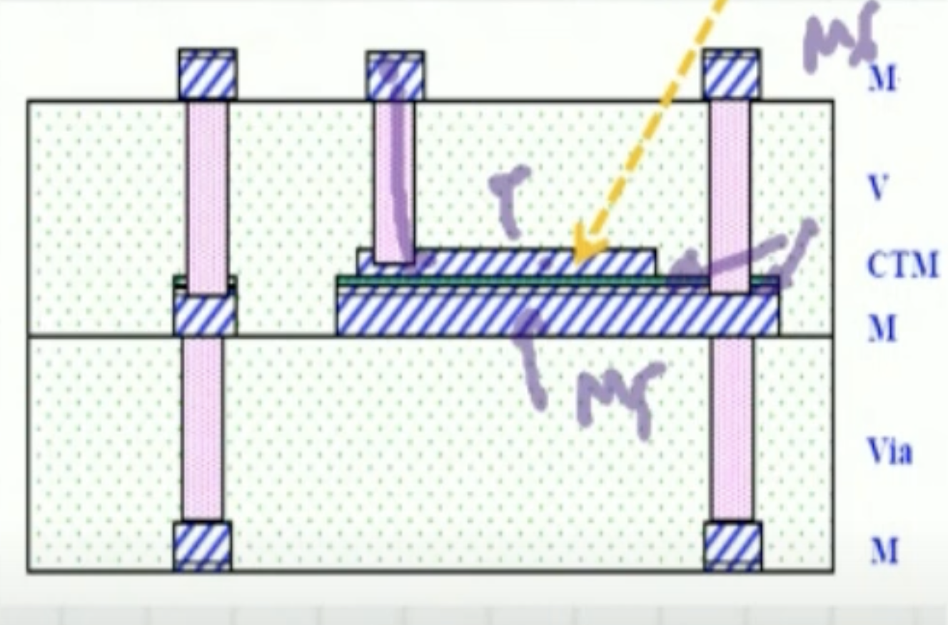
- 加上Contact, 目的是减小$d$, 增加电容大小
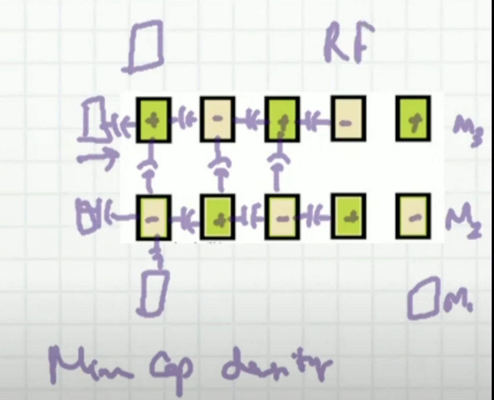
MoM (Metal-Oxide-Metal)
-
通过给不同的金属加上正负电,产生电容
-
氧化物可能附着在上层/下层金属,也有可能作为一个独立的介电层
-
不容易建模和预测
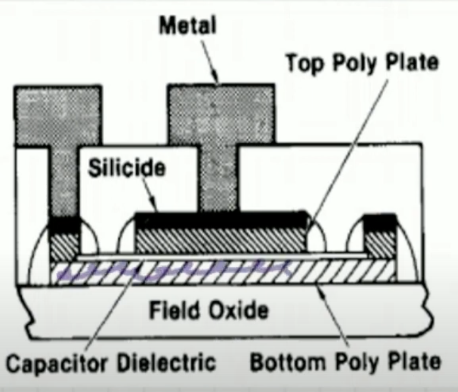
PiP (Poly-Insulator-Poly)
MOS (MOSFET Capacitor)
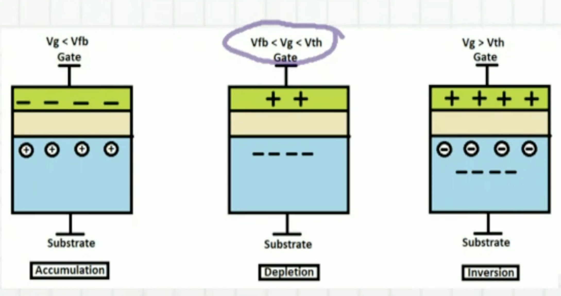
- $C_{ox} - V_{dc}$
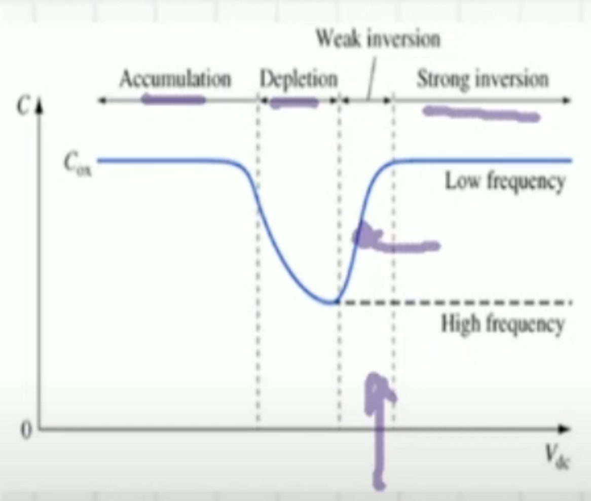
- Varactor
On-Chip Inductor
Basic Inductor
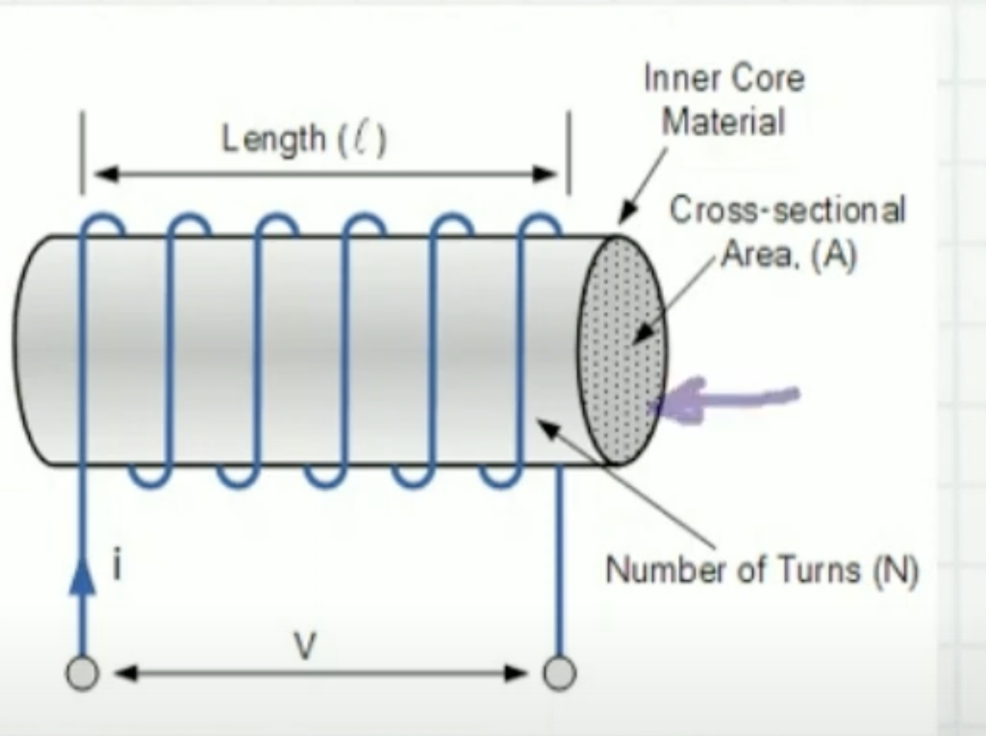
$$ \begin{gather} \begin{aligned} L &= \mu_0 \frac{ N^2 A }{ l } \\ \mu_0 &= 4\pi \times 10^{-7} \end{aligned} \end{gather} $$
On-Chip Inductor
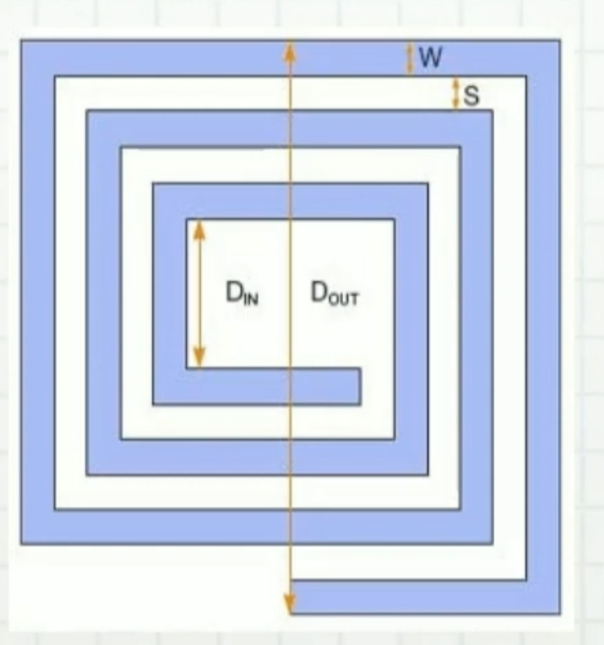
- Ideal Inductor is Circular